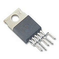
LM2592HVT-ADJ National Semiconductor, LM2592HVT-ADJ Datasheet - Page 16

LM2592HVT-ADJ
Manufacturer Part Number
LM2592HVT-ADJ
Description
Voltage Regulator IC
Manufacturer
National Semiconductor
Specifications of LM2592HVT-ADJ
Input Voltage
60V
Output Current
2A
Output Voltage
57V
No. Of Pins
5
Termination Type
Through Hole
Mounting Type
Through Hole
Voltage Regulator Type
Buck Switching
Output Current Max
2A
Lead Free Status / RoHS Status
Contains lead / RoHS non-compliant
Available stocks
Company
Part Number
Manufacturer
Quantity
Price
Company:
Part Number:
LM2592HVT-ADJ
Manufacturer:
NS
Quantity:
500
www.national.com
Application Information
sion. Since this regulator topology can produce an output
voltage that is either greater than or less than the input
voltage, the maximum output current greatly depends on
both the input and output voltage.
To determine how much load current is possible before the
internal device current limit is reached (and power limiting
occurs), the system must be evaluated as a buck-boost
configuration rather than as a buck. The peak switch current
in Amperes, for such a configuration is given as:
where L is in µH and f is in Hz. The maximum possible load
current I
While checking for this, take I
current limit value (min across tolerance and temperature is
2.3A for the LM2592HV). Also to account for inductor toler-
ances, we should take the min value of Inductance for L in
the equation above (typically 20% less than the nominal
value). Further, the above equation disregards the drop
across the Switch and the diode. This is equivalent to as-
This circuit has hysteresis
C
C
IN
OUT
Regulator starts switching at V
Regulator stops switching at V
470 µF/50V Elec. Panasonic HFQ
220 µF/25V Elec. Panasonic HFQ
— 68 µF/25V Tant. Sprague 595D
— 47 µF/20V Tant. Sprague 595D
LOAD
is limited by the requirement that I
FIGURE 10. Undervoltage Lockout with Hysteresis for Inverting Regulator
CLIM
FIGURE 11. Inverting −5V Regulator with Delayed Startup
IN
IN
to be the lowest possible
= 13V
= 8V
(Continued)
PEAK
I
CLIM
.
16
suming 100% efficiency, which is never so. Therefore expect
I
the above equation.
The reader is also referred to Application Note AN-1157 for
examples based on positive to negative configuration.
The maximum voltage appearing across the regulator is the
absolute sum of the input and output voltage, and this must
be limited to a maximum of 60V. For example, when convert-
ing +20V to −12V, the regulator would see 32V between the
input pin and ground pin. The LM2592HV has a maximum
input voltage spec of 60V.
Additional diodes are required in this regulator configuration.
Diode D1 is used to isolate input voltage ripple or noise from
coupling through the C
or no load conditions. Also, this diode isolation changes the
topology to closley resemble a buck configuration thus pro-
viding good closed loop stability. A Schottky diode is recom-
mended for low input voltages, (because of its lower voltage
drop) but for higher input voltages, a fast recovery diode
could be used.
Without diode D3, when the input voltage is first applied, the
charging current of C
eral volts for a short period of time. Adding D3 prevents the
output from going positive by more than a diode voltage.
PEAK
to be an additional 10-20% higher than calculated from
IN
10129439
IN
can pull the output positive by sev-
capacitor to the output, under light
10129440


