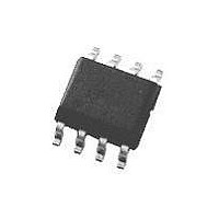
LM7372MR National Semiconductor, LM7372MR Datasheet - Page 10

LM7372MR
Manufacturer Part Number
LM7372MR
Description
Operational Amplifier (Op-Amp) IC
Manufacturer
National Semiconductor
Specifications of LM7372MR
Op Amp Type
High Speed
No. Of Amplifiers
2
Slew Rate
3000V/µs
No. Of Pins
8
Operating Temperature Range
-40°C To +85°C
Termination Type
SMD
Amplifier Type
Operational
Lead Free Status / RoHS Status
Contains lead / RoHS non-compliant
Available stocks
Company
Part Number
Manufacturer
Quantity
Price
Company:
Part Number:
LM7372MR
Manufacturer:
nstion
Quantity:
210
Part Number:
LM7372MR
Manufacturer:
NS/国半
Quantity:
20 000
www.national.com
Simplified Schematic Diagram
Application Notes
The LM7372 is a high speed dual operational amplifier with
a very high slew rate and very low distortion, yet like many
other op amps, it is used in conventional voltage feedback
amplifier applications. Also, again like many op amps, it has
a class AB output stage in order to be able to deliver high
currents to low impedance loads, yet draw very little quies-
cent supply current. For most op-amps in typical applica-
tions, this topology means that internal power dissipation is
rarely an issue, even with the trend to smaller surface mount
packages. However, the LM7372 has been designed for
applications where significant levels of power dissipation will
be encountered, and an effective means of removing the
internal heat generated by this power dissipation is needed
to maintain the semiconductor junction temperature at ac-
ceptable levels, particularly in environments with elevated
ambient temperatures.
Several factors contribute to power dissipation and conse-
quently higher semiconductor junction temperatures, and
these factors need to be well understood if the LM7372 is to
perform to the desired specifications in a given application.
Since different applications will have different dissipation
levels and different compromises can be made between the
ways these factors will contribute to the total junction tem-
perature, this section will examine the typical application
shown on the front page of this data sheet as an example,
and offer suggestions for solutions where excessive junction
temperatures are encountered.
There are two major contributors to the internal power dissi-
pation; the product of the supply voltage and the LM7372
quiescent current when no signal is being delivered to the
external load, and the additional power dissipated while
delivering power to the external load. The first of these
components is easy to calculate simply by inspection of the
data sheet. The LM7372 quiescent supply current is given as
6.5mA per amplifier, so with a 24Volt supply the power
dissipation is
10
This is already a high level of internal power dissipation, and
in a small surface mount package with a thermal resistance
(
package) would result in a junction temperature 140˚C/W x
0.312W = 43.7˚C above the ambient temperature. A similar
calculation using the worst case maximum current limit at an
85˚C ambient will yield a power dissipation of 456mW with a
junction temperature of 149˚C, perilously close to the maxi-
mum permitted junction temperature of 150˚C!
The second contributor to high junction temperature is the
additional power dissipated internally when power is being
delivered to the external load. This cause of temperature rise
can be less amenable to calculation, even when the actual
operating conditions are known.
For a Class B output stage, one transistor of the output pair
will conduct the load current as the output voltage swings
positive, with the other transistor drawing no current, and
hence dissipating no power. During the other half of the
signal swing this situation is reversed, with the lower transis-
tor sinking the load current and the upper transistor is cut off.
The current in each transistor will be a half wave rectified
version of the total load current. Ideally neither transistor will
dissipate power when there is no signal swing, but will
dissipate increasing power as the output current increases.
However, as the signal voltage across the load increases
with load current, the voltage across the output transistor
(which is the difference voltage between the supply voltage
and the instantaneous voltage across the load) will decrease
and a point will be reached where the dissipation in the
transistor will begin to decrease again. If the signal is driven
into a square wave, ideally the transistor dissipation will fall
all the way back to zero.
JA
= 140˚C/Watt (a not unreasonable value for an SO-8
PQ = V
= 24 x (6.5 x 10-3)
= 312mW
S
x 2Iq
(V
S
= V
CC
+ V
20004928
EE
)


