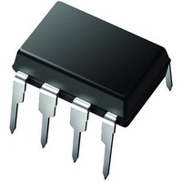
PIC12CE674-04E/P Microchip Technology, PIC12CE674-04E/P Datasheet - Page 23

PIC12CE674-04E/P
Manufacturer Part Number
PIC12CE674-04E/P
Description
IC,MICROCONTROLLER,8-BIT,PIC CPU,CMOS,DIP,8PIN,PLASTIC
Manufacturer
Microchip Technology
Series
PIC® 12Cr
Datasheets
1.PIC16F688T-ISL.pdf
(688 pages)
2.PIC12CE673-10P.pdf
(129 pages)
3.PIC12CE673-10P.pdf
(3 pages)
4.PIC12CE673-10P.pdf
(14 pages)
5.PIC12CE673-10P.pdf
(12 pages)
Specifications of PIC12CE674-04E/P
Rohs Compliant
YES
Core Processor
PIC
Core Size
8-Bit
Speed
4MHz
Peripherals
POR, WDT
Number Of I /o
5
Program Memory Size
3.5KB (2K x 14)
Program Memory Type
OTP
Eeprom Size
16 x 8
Ram Size
128 x 8
Voltage - Supply (vcc/vdd)
3 V ~ 5.5 V
Data Converters
A/D 4x8b
Oscillator Type
Internal
Operating Temperature
-40°C ~ 125°C
Package / Case
8-DIP (0.300", 7.62mm)
Processor Series
PIC12C
Core
PIC
Data Bus Width
8 bit
Data Ram Size
128 B
Maximum Clock Frequency
4 MHz
Number Of Programmable I/os
5
Number Of Timers
8
Maximum Operating Temperature
+ 125 C
Mounting Style
Through Hole
3rd Party Development Tools
52715-96, 52716-328, 52717-734
Development Tools By Supplier
ICE2000
Minimum Operating Temperature
- 40 C
On-chip Adc
8 bit
Lead Free Status / RoHS Status
Lead free / RoHS Compliant
Connectivity
-
Lead Free Status / Rohs Status
Details
Available stocks
Company
Part Number
Manufacturer
Quantity
Price
Company:
Part Number:
PIC12CE674-04E/P
Manufacturer:
MICROCHIP
Quantity:
12 000
4.5
The INDF Register is not a physical register. Address-
ing the INDF Register will cause indirect addressing.
Any instruction using the INDF register actually
accesses the register pointed to by the File Select Reg-
ister, FSR. Reading the INDF Register itself indirectly
(FSR = ’0’) will read 00h. Writing to the INDF Register
indirectly results in a no-operation (although status bits
may be affected). An effective 9-bit address is obtained
by concatenating the 8-bit FSR Register and the IRP bit
(STATUS<7>), as shown in Figure 4-4. However, IRP is
not used in the PIC12C67X.
A simple program to clear RAM locations 20h-2Fh
using indirect addressing is shown in Example 4-1.
FIGURE 4-4:
1999 Microchip Technology Inc.
RP1 RP0
bank select
For register file map detail see Figure 4-2.
Note 1: The RP1 and IRP bits are reserved; always maintain these bits clear.
Indirect Addressing, INDF and FSR
Registers
(1)
location select
6
Direct Addressing
DIRECT/INDIRECT ADDRESSING
Data
Memory
from opcode
7Fh
00h
Bank 0
00
0
Bank 1
01
Bank 2
10
not used
EXAMPLE 4-1:
NEXT
CONTINUE
Bank 3
11
movlw
movwf
clrf
incf
btfss
goto
:
IRP
bank select
180h
1FFh
(1)
0x20
FSR
INDF
FSR,F
FSR,4
NEXT
INDIRECT ADDRESSING
7
Indirect Addressing
PIC12C67X
;initialize pointer
;to RAM
;clear INDF register
;inc pointer
;all done?
;no clear next
;yes continue
FSR register
DS30561B-page 23
location select
0


