US4881EUA Melexis Inc, US4881EUA Datasheet
US4881EUA
Specifications of US4881EUA


Related parts for US4881EUA


US4881EUA Summary of contents
Page 1
Features and Benefits Operating voltage range from 2.2V to 18V Very high magnetic sensitivity CMOS technology Chopper-stabilized amplifier stage Low current consumption Open drain output Thin SOT23 3L and flat TO-92 3L both RoHS Compliant packages Ordering Information Part No. ...
Page 2
Table of Contents 1 Functional Diagram ........................................................................................................ 1 2 General Description........................................................................................................ 1 3 Glossary of Terms .......................................................................................................... 3 4 Absolute Maximum Ratings ........................................................................................... 3 5 Pin Definitions and Descriptions................................................................................... 3 6 General Electrical Specifications .................................................................................. 4 7 Magnetic Specifications ................................................................................................. ...
Page 3
Glossary of Terms MilliTesla (mT), Gauss Units of magnetic flux density: 1mT = 10 Gauss RoHS Restriction of Hazardous Substances TSOT Thin Small Outline Transistor (TSOT package) – also referred with the Melexis package code “SE” ESD Electro-Static Discharge ...
Page 4
General Electrical Specifications DC Operating Parameters Parameter Table 3: Electrical specifications 7 Magnetic Specifications DC Operating Parameters T = 25º Parameter Symbol Table 4: Magnetic specifications Note: For typical values, please refer to ...
Page 5
Detailed General Description Based on mixed signal CMOS technology, Melexis US4881 is a Hall-effect device with very high magnetic sensitivity. It allows using generic magnets, weak magnets or larger air gap. The chopper-stabilized amplifier uses switched capacitor technique to ...
Page 6
Performance Graphs 11.1 Magnetic parameters vs Bop, VDD=3V Brp, VDD=3V Bop, VDD=5V Brp, VDD=5V 4 Bop, VDD=12V Brp, VDD=12V -40 - (° C) 11.3 V vs. T ...
Page 7
I vs. T OFF VDD=3V VDD=5V 20 VDD=12V -40 - (° Test Conditions Note : DUT = Device Under Test 12.1 Supply Current 12.3 Output ...
Page 8
Application Information 13.1 Typical Three-Wire Application Circuit 13.3 Automotive and Harsh, Noisy Environments Three-Wire Circuit 13.4 Application Comments For proper operation, a 100nF bypass capacitor should be placed as close as possible to the device between the V and ...
Page 9
Standard information regarding manufacturability of Melexis products with different soldering processes Our products are classified and qualified regarding soldering technology, solderability and moisture sensitivity level according to following test methods: Reflow Soldering SMD’s (Surface Mount Devices) IPC/JEDEC J-STD-020 • ...
Page 10
Package Information 16.1 SE Package (TSOT-3L) see note 2 TOP VIEW see note 5 END VIEW TOP VIEW 3901004881 Rev 012 Low Voltage & Very High Sensitivity SIDE VIEW SECTION B-B’ see note 6 Hall plate location END VIEW ...
Page 11
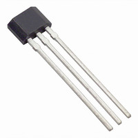
UA Package (TO-92 flat) 3901004881 Rev 012 Low Voltage & Very High Sensitivity Hall plate location Page US4881 Bipolar Hall Switch Data Sheet Jan/07 ...
Page 12
Disclaimer Devices sold by Melexis are covered by the warranty and patent indemnification provisions appearing in its Term of Sale. Melexis makes no warranty, express, statutory, implied description regarding the information set forth herein or regarding the ...