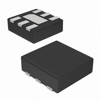
ISL29003IROZ-T7 Intersil, ISL29003IROZ-T7 Datasheet - Page 6

ISL29003IROZ-T7
Manufacturer Part Number
ISL29003IROZ-T7
Description
IC SENSOR LIGHT-DGTL I2C 6-ODFN
Manufacturer
Intersil
Datasheet
1.ISL29003IROZ-EVALZ.pdf
(15 pages)
Specifications of ISL29003IROZ-T7
Wavelength
540nm
Output Type
I²C™
Package / Case
6-ODFN
Lead Free Status / RoHS Status
Lead free / RoHS Compliant
Other names
ISL29003IROZ-T7TR
Available stocks
Company
Part Number
Manufacturer
Quantity
Price
Company:
Part Number:
ISL29003IROZ-T7
Manufacturer:
INTERSIL
Quantity:
1 831
Command Register 00(hex)
The Read/Write command register has five functions:
For proper shut down operation, it is recommended to
disable ADC first then disable the chip. Specifically, the user
should first send I
I
2
b1xxx_xxxx
bx1xx_xxxx
1. Enable; Bit 7. This function either resets the ADC or
2. ADCPD; Bit 6. This function puts the device in a
3. Timing Mode; Bit 5. This function determines whether the
4. Photodiode Select Mode; Bits 3 and 2. This function
ADDRESS
C command with Bit 6 = 1.
enables the ADC in normal operation. A logic 0 disables
ADC to reset-mode. A logic 1 enables adc to normal
operation.
power-down mode. A logic 0 puts the device in normal
operation. A logic 1 powers down the device.
integration time is done internally or externally. In Internal
Timing Mode, integration time is determined by an
internal dual speed oscillator (f
8, 12,16) counter inside the ADC. In External Timing
Mode, integration time is determined by the time between
two consecutive external-sync sync_iic pulse commands.
controls the mux attached to the two photodiodes. At
Mode1, the mux directs the current of Diode1 to the ADC.
BIT 5
BIT 7
BIT 6
0
1
0
1
0
1
TABLE 2. WRITE ONLY REGISTERS
Internal Timing Mode. Integration time is internally
timed determined by f
clock cycles.
External Timing Mode. Integration time is externally
timed by the I
REGISTER
Disable ADC-Core to Reset-Mode (default)
Enable ADC-Core to Normal Operation
Normal Operation (default)
Power-Down
sync_iic
clar_int
NAME
2
TABLE 5. TIMING MODE
C command with Bit 7 = 0 and then send
TABLE 3. ENABLE
TABLE 4. ADCPD
2
C host.
Writing a logic 1 to this address bit
ends the current ADC-integration
and starts another. Used only with
External Timing Mode.
Writing a logic 1 to this address bit
clears the interrupt.
6
OPERATION
OPERATION
OPERATION
OSC
OSC
DESCRIPTION
, REXT, and number of
FUNCTIONS/
), and the n-bit (n = 4,
ISL29003
*n = 4, 8, 12,16 depending on the number of clock cycles
function.
Control Register 01(hex)
The Read/Write control register has three functions:
5. Width; Bits 1 and 0. This function determines the number
1. Interrupt flag; Bit 5. This is the status bit of the interrupt.
2. Range/Gain; Bits 3 and 2. The Full Scale Range can be
BITS 3:2
BITS 1:0
At Mode2, the mux directs the current of Diode2 only to
the ADC. Mode3 is a sequential Mode1 and Mode2 with
an internal subtract function (Diode1 - Diode2).
of clock cycles per conversion. Changing the number of
clock cycles does more than just change the resolution of
the device; it also changes the integration time, which is
the period the device’s analog-to-digital (A/D) converter
samples the photodiode current signal for a lux
measurement.
The bit is set to logic high when the interrupt thresholds
have been triggered, and logic low when not yet
triggered. Writing a logic low clears/resets the status bit.
adjusted by an external resistor R
adjusted via I
Gain/Range has four possible values, Range(k) where k
is 1 through 4. Table 9 lists the possible values of
Range(k) and the resulting FSR for some typical value
R
TABLE 6. PHOTODIODE SELECT MODE; BITS 2 AND 3
BIT 5
0:0
0:1
1:0
1:1
EXT
0:0
0:1
1:0
1:1
0
1
resistors.
MODE1. ADC integrates or converts Diode1 only.
Current is converted to an n-bit unsigned data.*
MODE2. ADC integrates or coverts Diode2 only.
Current is converted to an n-bit unsigned data.*
MODE3. A sequential MODE1 then MODE2
operation. The difference current is an (n-1) signed
data.*
No Operation.
2
2
2
2
Interrupt is cleared or not triggered yet
Interrupt is triggered
TABLE 8. INTERRUPT FLAG
16
12
8
4
2
C using the Gain/Range function.
= 256
= 16
= 65,536
= 4,096
TABLE 7. WIDTH
NUMBER OF CLOCK CYCLES
OPERATION
MODE
EXT
and/or it can be
August 8, 2008
FN7464.5


