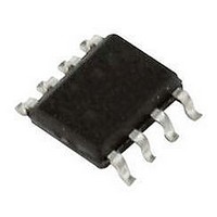
SRDA05-6.T Semtech, SRDA05-6.T Datasheet - Page 5

SRDA05-6.T
Manufacturer Part Number
SRDA05-6.T
Description
TVS DIODE ARRAY, 500W, 5V, SOIC
Manufacturer
Semtech
Datasheet
1.SRDA05-6.T.pdf
(9 pages)
Specifications of SRDA05-6.T
Diode Type
Low Capacitance
Clamping Voltage Vc Max
20V
Operating Voltage
1.5V
Diode Case Style
SOIC
No. Of Pins
8
Peak Pulse Power Ppk @ 8x20us
500W
Junction Capacitance
15pF
Breakdown Voltage Min
6V
Breakdown Voltage Vbr
6V
Capacitance, Cd
4pF
Rohs Compliant
Yes
Lead Free Status / RoHS Status
Lead free / RoHS Compliant
Available stocks
Company
Part Number
Manufacturer
Quantity
Price
Part Number:
SRDA05-6.TB
Manufacturer:
SEMTECH/美国升特
Quantity:
20 000
Company:
Part Number:
SRDA05-6.TBT
Manufacturer:
SEMTECH
Quantity:
367
Part Number:
SRDA05-6.TBT
Manufacturer:
SEMTECH/美国升特
Quantity:
20 000
Part Number:
SRDA05-6.TE
Manufacturer:
SEMTECH/美国升特
Quantity:
20 000
Device Connection Options for Protection of Six High-
Speed Lines
The SRDA TVS is designed to protect four data lines
from transient overvoltages by clamping them to a
fixed reference. When the voltage on the protected
line exceeds the reference voltage (plus diode V
steering diodes are forward biased, conducting the
transient current away from the sensitive circuitry.
Data lines are connected at pins 1, 2, 4, 5, 6 and 7.
The negative reference is connected at pin 8. These
pins should be connected directly to a ground plane on
the board for best results. The path length is kept as
short as possible to minimize parasitic inductance.
The positive reference is connected at pins 2 and 3.
In the case of the SRDA3.3-6, pins 2 and 3 are
connected internally to the cathode of the low voltage
TVS. It is not recommended that these pins be directly
connected to a DC source greater than the snap-back
votlage (V
below.
EPD TVS Characteristics
These devices are constructed using Semtech’s
proprietary EPD technology. By utilizing the EPD tech-
nology, the SRDA3.3-6 can effectively operate at 3.3V
while maintaining excellent electrical characteristics.
The EPD TVS employs a complex nppn structure in
contrast to the pn structure normally found in tradi-
tional silicon-avalanche TVS diodes. Since the EPD
TVS devices use a 4-layer structure, they exhibit a
slightly different IV characteristic curve when compared
to conventional devices. During normal operation, the
device represents a high-impedance to the circuit up to
the device working voltage (V
event, the device will begin to conduct and will enter a
low impedance state when the punch through voltage
(V
voltage TVS will exhibit a slight negative resistance
characteristic as it conducts current. This characteris-
tic aids in lowering the clamping voltage of the device,
but must be considered in applications where DC
voltages are present.
When the TVS is conducting current, it will exhibit a
slight “snap-back” or negative resistance characteris-
tics due to its structure. This point is defined on the
PROTECTION PRODUCTS
PROTECTION PRODUCTS
© 2010 Semtech Corp.
Applications Information
PT
) is exceeded. Unlike a conventional device, the low
SB
) as the device can latch on as described
RWM
). During an ESD
F
) the
5
Data Line Protection Using Internal TVS Diode as
Reference
curve by the snap-back voltage (V
current (I
current through the device must fall below the I
(approximately <50mA) and the voltage must fall below
the V
TVS is connected to 3.3V DC source, it will never fall
below the snap-back voltage of 2.8V and will therefore
stay in a conducting state.
SB
V
BRR
SRDA3.3-6 and SRDA05-6
(normally 2.8 volts for a 3.3V device). If a 3.3V
SB
). To return to a non-conducting state, the
EPD TVS IV Characteristic Curve
I
I
I
I
SB
PT
PP
R
I
BRR
SB
) and snap-back
V
RWM
www.semtech.com
V
SB
V
PT
V
C
SB


