HDLU-1414 Avago Technologies US Inc., HDLU-1414 Datasheet - Page 7
HDLU-1414
Manufacturer Part Number
HDLU-1414
Description
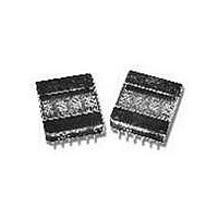
Smart 5 X 7 Dot Matrix LED Display,4-CHARACTER,Red,DIP
Manufacturer
Avago Technologies US Inc.
Series
HDLx-1414r
Datasheet
1.HDLY-1414.pdf
(9 pages)
Specifications of HDLU-1414
Millicandela Rating
*
Internal Connection
*
Size / Dimension
0.70" L x 0.80" W x 0.24" H (17.7mm x 20.1mm x 6.1mm)
Color
Red
Configuration
*
Voltage - Forward (vf) Typ
*
Package / Case
12-DIP
Display Type
Alphanumeric
Number Of Digits/alpha
4
Digit/alpha Size
0.14" (3.6mm)
Number Of Digits
4
Illumination Color
Red
Wavelength
637 nm
Operating Voltage
5 V
Maximum Operating Temperature
+ 85 C
Minimum Operating Temperature
- 40 C
Luminous Intensity
3.1 mcd
Lead Free Status / RoHS Status
Lead free / RoHS Compliant
Common Pin
-
Lead Free Status / Rohs Status
Details


7
Electrical Description
Pin Function
\Write (\WR, Pin 3)
Address Inputs
(A
V
Ground (GND, Pin 7)
Data Inputs
(D0–D6, Pins 1, 2, 8-12)
Figure 1. Display truth table.
Display Internal Block Diagram
Figure 2 shows the HDLX-1414
display internal block diagram.
The CMOS IC consists of a 4 x 7
Character RAM, a 128-character
ASCII decoder and the refresh
circuitry necessary to
synchronize the decoding and
driving of four 5 x 7 dot matrix
characters.
Four 7-bit ASCII words are
stored in the Character RAM.
The IC reads the ASCII data and
decodes it vita the 128-character
ASCII decoder. This decoder
includes the 64-character set of
the HPDL-1414, 32 lower case
ASCII symbols, and 32 foreign
language symbols.
DD
\
1
WR
1
0
0
0
0
and A
(Pin 6)
A1
0
X
0
0
1
1
, Pins 4 and 5)
A0
X
0
1
0
1
D6
Digit 0 ASCII Data (Right Most
Character)
Digit 1 ASCII Data
Digit 2 ASCII Data
Digit 3 ASCII Data (Left Most
Character)
X
D5
X
0 = Logic 0; 1 = Logic 1; X = Do Not Care.
Description
WR must be logic 0 to store data in the display.
A
memory. Address 00 accesses the far right
character, and address 11 accesses the far left
position.
V
Ground is the display ground.
D0–D6 are used to specify the input data for
the display.
DD
0
D4
and A
X
is the positive power supply input.
1
D3
X
select a specific location in the display
Data Entry
Figure 1 shows a truth table for
the HDLX-1414 display. Address
inputs A
select the digit location in the
display. When A
both logic low, data is loaded
into the right most character.
Data inputs D
load information into the
display. Data is latched into the
given character address on the
rising edge of the \WR signal.
Data and Address inputs must
be held stable during the write
cycle to ensure that correct data
is stored in the display.
D2
X
0
D1
X
and A
0
D0
–D
X
1
0
are used to
6
and A
are used to
No Change
Write to
Character
RAM
Function
1
are
Mechanical and Electrical
Considerations
The HDLX-1414 is a 12-pin DIP
package that can be stacked to
create a character array of any
size. The display is designed to
operate reliably in –40˚C to
+85˚C ambient temperatures.
The HDLX-1414 is assembled by
die attaching and wire bonding
140 LEDs and a CMOS IC to a
high temperature printed circuit
board. A polycarbonate lens is
placed over the PC board,
creating a protective air gap
over the LED wire bonds.
Backfill epoxy environmentally
seals the display package. This
package construction makes the
display highly tolerant to
temperature cycling and allows
wave soldering.
ESD and Latchup Protection
The inputs to the CMOS IC are
protected against static
discharge and input current
latchup. However, for best
results, standard CMOS handling
precautions should be used.
Prior to use, the HDLX-1414
should be stored in antistatic
tubes or conductive material.
During assembly a grounded
conductive work area should be
used, and assembly personnel
should wear conductive wrist
straps. Lab coats made of
synthetic material should be
avoided since they are prone to
static charge build-up. Input
current latchup can be caused
when the CMOS inputs are
subjected either to a voltage
below ground (V
higher than V
when a high current is forced
into the input. To prevent input
current latchup and ESD
damage, unused inputs should
be connected either to ground or
to V
DD
. Voltages should not be
DD
in
(V
< ground) or
in
> V
DD
) and
Related parts for HDLU-1414
Image
Part Number
Description
Manufacturer
Datasheet
Request
R

Part Number:
Description:
LED DISPLAY 5X7 4CHAR 5MM RED
Manufacturer:
Avago Technologies US Inc.
Datasheet:

Part Number:
Description:
OPTOCOUPLER GATE DRV 2A 16-SOIC
Manufacturer:
Avago Technologies US Inc.
Datasheet:
Part Number:
Description:
OPTOCOUPLER 2CH 2.5A 16-SOIC
Manufacturer:
Avago Technologies US Inc.
Datasheet:

Part Number:
Description:
OPTOCOUPLER GATE DRV 0.4A 16SOIC
Manufacturer:
Avago Technologies US Inc.
Datasheet:

Part Number:
Description:
OPTOCOUPLER 2.0A 250KHZ 8-DIP
Manufacturer:
Avago Technologies US Inc.
Datasheet:

Part Number:
Description:
OPTOCOUPLER 2.0A 250KHZ GW 8-SMD
Manufacturer:
Avago Technologies US Inc.
Datasheet:

Part Number:
Description:
OPTOCOUPLER 2CH 15MBD 3.3V 8SOIC
Manufacturer:
Avago Technologies US Inc.
Datasheet:
Part Number:
Description:
OPTOCOUPLER DARL-OUT 8-DIP
Manufacturer:
Avago Technologies US Inc.
Datasheet:
Part Number:
Description:
OPTOCOUPLER IGBT DRIVE 0.4A 8DIP
Manufacturer:
Avago Technologies US Inc.
Datasheet:
Part Number:
Description:
OPTOCOUPLER DARL-OUT 8-DIP
Manufacturer:
Avago Technologies US Inc.
Datasheet:

Part Number:
Description:
OPTOCOUPLER 1CH 1MBS 8-SMD GW
Manufacturer:
Avago Technologies US Inc.
Datasheet:
Part Number:
Description:
OPTOCOUPLER GATE DRIVER 8-DIP
Manufacturer:
Avago Technologies US Inc.
Datasheet:

Part Number:
Description:
OPTOCOUPLER GATE DRIVER 8-SMD
Manufacturer:
Avago Technologies US Inc.
Datasheet:

Part Number:
Description:
OPTOCOUPLER PHOTOTRANS 4-SMD
Manufacturer:
Avago Technologies US Inc.
Datasheet:

Part Number:
Description:
OPTOCOUPLER W/BASE 6-DIP
Manufacturer:
Avago Technologies US Inc.
Datasheet: