HV832MG Supertex, HV832MG Datasheet
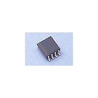
Display Drivers Dual HVCMOS

HV832MG

Manufacturer Part Number
HV832MG
Description
Display Drivers Dual HVCMOS
Manufacturer
Supertex
Datasheet

Specifications of HV832MG

Driver Type
EL Lamp Drivers
Maximum Operating Temperature
+ 85 C
Mounting Style
SMD/SMT
Package / Case
MSOP-8
Minimum Operating Temperature
- 40 C
Lead Free Status / RoHS Status
Lead free / RoHS Compliant
Features
Applications
Typical Application Circuit
Patented audible noise reduction
Patented lamp aging compensation
210 V
Patented output timing for high effi ciency
Single cell lithium ion compatible
150nA shutdown current
Wide input voltage range 1.8V to 5.0V
Separately adjustable lamp and converter
frequencies
Output voltage regulation
Split supply capability
LCD backlighting
Mobile Cellular Phone keypads
PDAs
Handheld wireless communication products
Global Positioning Systems (GPS)
PP
output voltage for higher brightness
V
Logic Input Pulse
IN
+
_
V
DD
High Voltage Dual EL Lamp Driver
C
IN
for Low Noise Applications
1
2
3
4
General Description
The Supertex HV832 is a high voltage driver designed for driving two
EL lamps with a combined area of 3.5in
range is from 2.0V to 5.0V. The device is designed to reduce the
amount of audible noise emitted by the lamp. It uses a single inductor
and a minimum number of passive components. The nominal
regulated output voltage that is applied to the EL lamp is ±90V.
The HV832 has an internal oscillator, a switching MOSFET, and
two high voltage EL lamp drivers. The frequency for the switching
MOSFET is set at 51KHz nominal. The EL lamp driver frequency is
set by dividing the MOSFET switching frequency by 128. An external
inductor is connected between the LX and VDD or VIN pins for split
supply applications. A 0.001 to 0.01µF, 100V capacitor is connected
between the CS pin and Ground. The EL lamps are connected
between EL1 to Com and EL2 to Com.
An input control pin is available to select various modes of the device.
Each logic pulse applied to the control pin will cause the device to
change to the next mode. The sequence for the modes is: (1) EL1 on
only, (2) EL2 on only, (3) both EL1 and EL2 on, and (4) device shuts
down. During power up of the device, the mode will default to shut
down.
The switching MOSFET charges the external inductor and discharges
it into the capacitor at CS. The voltage at CS will start to increase.
Once the voltage at CS reaches a nominal value of 90V, the switching
MOSFET is turned off to conserve power. The outputs EL1 to Com
and EL2 to Com are confi gured as H bridges EL1/EL2 and Com
and are switching in opposite states to achieve 180V across the EL
lamp.
EL1
VDD
Control
GND
HV832MG
Com
EL2
CS
LX
8
7
6
5
L
X
EL Lamp 1
C
S
2
. The input supply voltage
EL Lamp 2
HV832

Related parts for HV832MG

HV832MG Summary of contents

Page 1

... MOSFET is turned off to conserve power. The outputs EL1 to Com and EL2 to Com are confi gured as H bridges EL1/EL2 and Com and are switching in opposite states to achieve 180V across the EL lamp. EL1 1 EL2 VDD Com Control 4 GND LX HV832MG The input supply voltage EL Lamp Lamp HV832 ...

Page 2

... Logic input low voltage IL V Logic input high voltage IH * The inductor used is a 220µH Murata inductor, max DC resistance of 8.4Ω, part # LQH32CN221K21. 1 MSOP-8 HV832MG-G Pin Confi guration Value -0.5V to 7.5V -0.5V to 125V -40°C to +85°C -65°C to +150°C 300mW ...

Page 3

... DD Control Control Logic & Switch Osc GND Function Table Control Pin EL1 Power up HI-Z 1 pulse pulse HI pulse pulse HI-Z TH Typical Performance Device Lamp HV832MG Both EL and SEN + C _ Disable V REF EL Osc = Switch Osc 128 EL2 HI 27mA 3.0V ON 38mA 3 HV832 ...

Page 4

... V (V) IN Brightness 1.5 2.5 3 EL1 1 EL2 8 VDD Com Control 4 GND LX 5 HV832MG L = 330µH Murata (LQH32CN331 any (equivalent or better) >90V, fast reverse recovery diode (one output on, EL Lamp = 1.5in I V Brightness vs. Inductor Value , , 200 300 400 Inductor Value ( 4 4.5 5 ...

Page 5

... EL1 1 EL2 VDD Com Control 4 GND HV832MG used to boost the low input voltage by inductive fl yback. When the internal switch The energy stored in the capacitor is connected to the will also increase. If the input power is greater than the power ...

Page 6

... JEDEC Registration MO-187, Variation AA, Issue E, Dec. 2004. Drawings not to scale. (The package drawing(s) in this data sheet may not refl ect the most current specifi cations. For the latest package outline information go to http://www.supertex.com/packaging.html.) Doc.# DSFP-HV832 A111306 E E1 ...

Related keywords