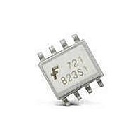
FOD0721 Fairchild Semiconductor, FOD0721 Datasheet - Page 2

FOD0721
Manufacturer Part Number
FOD0721
Description
High Speed Optocouplers High CMR 25Mbit/sec Logic Gate
Manufacturer
Fairchild Semiconductor
Datasheet
1.FOD0721.pdf
(12 pages)
Specifications of FOD0721
Isolation Voltage
3750 Vrms
Maximum Fall Time
4.5 ns
Maximum Rise Time
5 ns
Minimum Forward Diode Voltage
3750 Vrms
Output Device
Logic Gate Photo IC
Configuration
1 Channel
Maximum Baud Rate
25 MBps
Maximum Power Dissipation
90 mW
Maximum Operating Temperature
+ 100 C
Minimum Operating Temperature
- 40 C
Package / Case
SOIC-8 Wide
Lead Free Status / RoHS Status
Lead free / RoHS Compliant
Available stocks
Company
Part Number
Manufacturer
Quantity
Price
Part Number:
FOD0721R2
Manufacturer:
ON/ه®‰و£®ç¾ژ
Quantity:
20 000
©2004 Fairchild Semiconductor Corporation
FOD0721, FOD0720, FOD0710 Rev. 1.0.9
Pin Definitions
Absolute Maximum Ratings
Stresses exceeding the absolute maximum ratings may damage the device. The device may not function or be
operable above the recommended operating conditions and stressing the parts to these levels is not recommended.
In addition, extended exposure to stresses above the recommended operating conditions may affect device reliability.
The absolute maximum ratings are stress ratings only.
Recommended Operating Conditions
The Recommended Operating Conditions table defines the conditions for actual device operation. Recommended
operating conditions are specified to ensure optimal performance to the datasheet specifications. Fairchild does not
recommend exceeding them or designing to absolute maximum ratings.
• A 0.1µF bypass capacitor must be connected between pins 1 and 4, and 5 and 8
• Pin 3 must be left unconnected
V
Pin Number
Symbol
DD1
Symbol
T
t
T
T
T
V
V
V
PD1
PD2
V
r
OPR
OPR
V
, t
STG
, V
SOL
DD1
V
DD2
I
IH
I
IL
O
I
D
I
1
2
3
4
5
6
7
8
f
DD2
Ambient Operating Temperature
Supply Voltages
Logic High Input Voltage
Logic Low Input Voltage
Input Signal Rise and Fall Time
Storage Temperature
Operating Temperature
Lead Solder Temperature
Reflow Temperature Profile (Refer to Relow Profile)
Input Supply Voltage
Input Voltage
Input DC Current
Output Supply Voltage
Output Voltage
Average Output Current
Input Power Dissipation
Output Power Dissipation
Pin Name
GND1
GND2
V
V
NC
V
DD1
DD2
V
O
I
Parameter
Parameter
(T
Input Supply Voltage
Input Data
LED Anode – must be left unconnected
Input Ground
Output Ground
Output Data
Not Connected
Output Supply Voltage
A
= 25°C unless otherwise specified.)
2
Pin Function Description
Min.
-40
4.5
2.0
0
-0.5 to V
-0.5 to V
260 for 10 sec
-40 to +125
-40 to +100
-10 to +10
0 to 6.0
0 to 6.0
Value
10
90
70
DD1
DD2
+ 0.5
+ 0.5
Max.
+100
V
5.5
0.8
1.0
DD1
Units
www.fairchildsemi.com
mW
mW
mA
°C
°C
°C
mA
V
V
V
V
Unit
ms
°C
V
V
V


