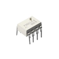
FOD2743BTV Fairchild Semiconductor, FOD2743BTV Datasheet
FOD2743BTV
Specifications of FOD2743BTV


Related parts for FOD2743BTV


FOD2743BTV Summary of contents
Page 1
... COMP 2 3 GND 4 FB ©2004 Fairchild Semiconductor Corporation FOD2743A, FOD2743B, FOD2743C Rev. 1.0.1 Description The FOD2743 Optically Isolated Amplifier consists of the popular KA431 precision programmable shunt reference and an optocoupler. The optocoupler is a gallium ars- enide (GaAs) light emitting diode optically coupled to a silicon phototransistor ...
Page 2
... Typical Application FAN4803 PWM V 1 Control ©2004 Fairchild Semiconductor Corporation FOD2743A, FOD2743B, FOD2743C Rev. 1.0.1 Pin Description Anode LED. This pin is the input to the light emitting diode. Error Amplifier Compensation. This pin is the output of the error amplifier. * Ground Voltage Feedback. This pin is the inverting input to the error amplifier ...
Page 3
... ECO I Collector Current C PD1 Input Power Dissipation PD2 Transistor Power Dissipation PD3 Total Power Dissipation Note: 1. See derating graph, Figure 21. ©2004 Fairchild Semiconductor Corporation FOD2743A, FOD2743B, FOD2743C Rev. 1.0 25°C unless otherwise specified) A Parameter (1) 3 Value Units -40 to +125 °C -40 to +85 ° ...
Page 4
... A 3. The dynamic impedance is defined as |Z resistors (see Figure 2), the total dynamic impedance of the circuit is given by ------- - Z 1 OUT, TOT OUT I ©2004 Fairchild Semiconductor Corporation FOD2743A, FOD2743B, FOD2743C Rev. 1.0 25°C unless otherwise specified) A Test Conditions I = 1mA (Fig.1) LED COMP FB ...
Page 5
... Vcm, to assure that the output will remain high. Common mode transient immunity at output low is the maximum tolerable (negative) dVcm/dt on the trailing edge of the common pulse signal,Vcm, to assure that the output will remain low. ©2004 Fairchild Semiconductor Corporation FOD2743A, FOD2743B, FOD2743C Rev. 1.0.1 (Continued 25° ...
Page 6
... REF 3 Figure (min.) Test Circuit REF F, LED I (LED REF Figure 3. I Test Circuit REF Figure 5. I Test Circuit CEO ©2004 Fairchild Semiconductor Corporation FOD2743A, FOD2743B, FOD2743C Rev. 1.0 Figure (LED) I CEO (LED COMP R2 V REF Test Circuit REF / COMP I (OFF) ...
Page 7
... Test Circuits (Continued + OUT 2.2k V OUT ©2004 Fairchild Semiconductor Corporation FOD2743A, FOD2743B, FOD2743C Rev. 1.0 1mA 0 Figure 7. Frequency Response Test Circuit 0mA ( 1mA ( VCM _ + 10V P-P Figure 8. CMH and CML Test Circuit 0.47V A B www.fairchildsemi.com ...
Page 8
... T – AMBIENT TEMPERATURE ( C) A Fig. 12 – Off–State Current vs. Ambient Temperature 100 V = 37V -40 - – AMBIENT TEMPERATURE ( C) A ©2004 Fairchild Semiconductor Corporation FOD2743A, FOD2743B, FOD2743C Rev. 1.0.1 1 COMP 0.5 0.0 -0.5 -1.0 – Fig. 11 – Reference Current vs Ambient Temperature 4.0 3.5 3.0 2 ...
Page 9
... I – FORWARD CURRENT (mA) LED Fig. 18 – Collector Current vs. Collector Voltage – COLLECTOR-EMITTER VOLTAGE (V) CE ©2004 Fairchild Semiconductor Corporation FOD2743A, FOD2743B, FOD2743C Rev. 1.0.1 (Continued) Fig. 15 – Collector Current vs. Ambient Temperature 100 -40 Fig. 17 – Saturation Voltage vs. Ambient Temperature 0.26 0.24 0.22 0.20 ...
Page 10
... Typical Performance Curves ©2004 Fairchild Semiconductor Corporation FOD2743A, FOD2743B, FOD2743C Rev. 1.0.1 (Continued) Fig. 20 – Voltage Gain vs. Frequency 10V 10mA 500 1mA 2. 10mA -10 - 100 FREQUENCY (kHz) Fig. 21 – Package Power Dissipation vs Ambient Temperature 200 150 100 50 0 -40 - – AMBIENT TEMPERATURE ( C) 10 ...
Page 11
... OUT ---------------------------- - 1040 A R TOP ©2004 Fairchild Semiconductor Corporation FOD2743A, FOD2743B, FOD2743C Rev. 1.0.1 Compensation The compensation pin of the FOD2743 provides the opportunity for the designer to design the frequency response of the converter. A compensation network may be placed between the COMP pin and the FB pin. ...
Page 12
... MIN 0.022 (0.56) 0.016 (0.41) 0.100 (2.54) TYP Lead Coplanarity : 0.004 (0.10) MAX Note: All dimensions are in inches (millimeters) ©2004 Fairchild Semiconductor Corporation FOD2743A, FOD2743B, FOD2743C Rev. 1.0.1 0.4" Lead Spacing 0.200 (5.08) 0.140 (3.55) 15 MAX 0.300 (7.62) TYP 0.022 (0.56) 0.016 (0.41) 8-Pin DIP – ...
Page 13
... SDV Marking Information Definitions ©2004 Fairchild Semiconductor Corporation FOD2743A, FOD2743B, FOD2743C Rev. 1.0.1 Example Part Number FOD2743A Standard Through Hole FOD2743AS Surface Mount Lead Bend FOD2743ASD Surface Mount; Tape and Reel FOD2743AT 0.4" Lead Spacing FOD2743AV VDE0884 FOD2743ATV VDE0884; 0.4” Lead Spacing FOD2743ASV VDE0884 ...
Page 14
... ©2004 Fairchild Semiconductor Corporation FOD2743A, FOD2743B, FOD2743C Rev. 1.0 User Direction of Feed Description Tape Width Tape Thickness Sprocket Hole Pitch Sprocket Hole Diameter Sprocket Hole Location Pocket Location Pocket Pitch Pocket Dimensions Cover Tape Width Cover Tape Thickness Max. Component Rotation or Tilt Min ...
Page 15
... Reflow Profile • Peak reflow temperature • Time of temperature higher than 245°C • Number of reflows 300 250 200 150 100 50 ©2004 Fairchild Semiconductor Corporation FOD2743A, FOD2743B, FOD2743C Rev. 1.0.1 260°C (package surface temperature) 40 seconds or less Three 100 150 Time (s) Figure 22 ...
Page 16
... TRADEMARKS The following includes registered and unregistered trademarks and service marks, owned by Fairchild Semiconductor and/or its global subsidiaries, and is not intended exhaustive list of all such trademarks. Build it Now™ CorePLUS™ CorePOWER™ CROSSVOLT™ CTL™ Current Transfer Logic™ ...