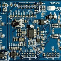
CDK-5560 Cirrus Logic Inc, CDK-5560 Datasheet

CDK-5560
Specifications of CDK-5560
Related parts for CDK-5560
CDK-5560 Summary of contents
Page 1
High-throughput Features Two Analog Input Channels Multiplexed to the CS5560 ADC Pre-configured to require a minimum number of external connections to your data acquisition system. All functionality accessible through the connector interface and board-level ...
Page 2
INTRODUCTION ....................................................................................................................... 3 1.1 Overview ............................................................................................................................ 4 2. QUICK START .......................................................................................................................... 5 3. HARDWARE DESCRIPTION ................................................................................................... 6 3.1 Absolute Maximum Ratings ............................................................................................... 6 3.2 Power Supply ..................................................................................................................... 6 3.3 Analog Section ................................................................................................................... 6 3.3.1 Analog Input Buffers .............................................................................................. 6 ...
Page 3
INTRODUCTION The CDB5560 evaluation board is a platform for evaluating the CS5560 ADC performance. The evalua- tion board is designed to connect to the SPI serial port of a processor or data capture system or will inter- face directly ...
Page 4
Overview The CDB5560 evaluation board has both analog and digital circuit sections. The analog section consists of the CS5560 ADC, two analog input signal buffers, controlled through a multiplexer, that condition the signals into the ADC, and a precision ...
Page 5
QUICK START Buffer Enable ADC Reset DC Supply NOTES: 1. Shaded boxes marked with "OPT. CONFIG." are not necessary for operation in an end user product. 2. Calibration function has been removed from the device but still appears on ...
Page 6
HARDWARE DESCRIPTION 3.1 Absolute Maximum Ratings Observe the following limits to ensure the CDB5560 component ratings are not exceeded. • CS5560 – The absolute maximum supply voltage that can be applied to the +3.3V power supply connection is +3.6V. ...
Page 7
For detailed information on the LMP7732 precision industrial op-amps, please visit National Semiconduc- tor’s website at www.national.com. The analog inputs are designed for connections to differential input signals. The usable input voltage range is -4.096 V to +4.096 V. The ...
Page 8
Digital Section 3.4.1 Hardware Configuration The CDB5560 evaluation board hardware comes pre-configured so the only connection required between it and a data acquisition system is the serial port connection. The hardware setup is reconfigurable through the hardware control interface ...
Page 9
APPENDIX A. MAXIMIZING THE PERFORMANCE OF THE CS5560 A.1 PCB Layout Considerations • Keep the signal path short between the CS5560 ADC input capacitors C20, C28, C37, C44 and the ADC input pins to minimize trace inductance. • The analog ...
Page 10
APPENDIX B. BILL OF MATERIALS 10 CDB5560 DS713DB4 ...
Page 11
APPENDIX C. SCHEMATICS DS713DB4 CDB5560 11 ...
Page 12
CDB5560 DS713DB4 ...
Page 13
DS713DB4 CDB5560 13 ...
Page 14
CDB5560 DS713DB4 ...
Page 15
DS713DB4 CDB5560 15 ...
Page 16
APPENDIX D. LAYER PLOTS 16 CDB5560 DS713DB4 ...
Page 17
DS713DB4 CDB5560 17 ...
Page 18
CDB5560 DS713DB4 ...
Page 19
DS713DB4 CDB5560 19 ...
Page 20
CDB5560 DS713DB4 ...
Page 21
DS713DB4 CDB5560 21 ...
Page 22
CDB5560 DS713DB4 ...
Page 23
DS713DB4 CDB5560 23 ...
Page 24
CDB5560 DS713DB4 ...
Page 25
APPENDIX E. CALIBRATION FUNCTION The calibration function has been removed from the CS5560. All references to calibration have been re- moved from this document. However, calibration still appears on the PCB. A jumper must be added to J2 for proper ...
Page 26
REVISION HISTORY Revision Date DB1 APR 2007 DB2 JUN 2007 DB3 DEC 2007 DB4 OCT 2009 Contacting Cirrus Logic Support For all product questions and inquiries contact a Cirrus Logic Sales Representative. To find the one nearest to you go ...


