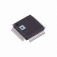
AD1833AASTZ Analog Devices Inc, AD1833AASTZ Datasheet - Page 14

AD1833AASTZ
Manufacturer Part Number
AD1833AASTZ
Description
6 Channel 24 Bit 192 KHz DAC I.C.
Manufacturer
Analog Devices Inc
Datasheet
1.AD1833ACSTZ.pdf
(20 pages)
Specifications of AD1833AASTZ
Number Of Bits
24
Data Interface
DSP, I²S, Serial
Number Of Converters
6
Voltage Supply Source
Analog and Digital
Operating Temperature
-40°C ~ 85°C
Mounting Type
Surface Mount
Package / Case
48-LQFP
Lead Free Status / RoHS Status
Lead free / RoHS Compliant
Power Dissipation (max)
-
Settling Time
-
Lead Free Status / RoHS Status
Lead free / RoHS Compliant
Available stocks
Company
Part Number
Manufacturer
Quantity
Price
Company:
Part Number:
AD1833AASTZ
Manufacturer:
Analog Devices Inc
Quantity:
10 000
Company:
Part Number:
AD1833AASTZ-REEL
Manufacturer:
Analog Devices Inc
Quantity:
10 000
AD1833A
I
I
mitted is for the left channel and when it is for the right channel.
The L/RCLK is low for the left channel and high for the right
channel. A bit clock running at 64
There is a delay of 1 bit clock from the time the L/RCLK signal
changes state to the first bit of data on the SDINx lines. The data
is written MSB first and is valid on the rising edge of the bit clock.
Left-Justified Timing
Left-justified (LJ) timing uses an L/RCLK to define when the
data being transmitted is for the left channel and when it is for
the right channel. The L/RCLK is high for the left channel and
low for the right channel. A bit clock running at 64
2
2
S Timing
S timing uses an L/RCLK to define when the data being trans-
L/RCLK
SDATA
L/RCLK
SDATA
L/RCLK
SDATA
INPUT
INPUT
INPUT
INPUT
INPUT
BCLK
INPUT
BCLK
INPUT
INPUT
INPUT
BCLK
LSB
MSB
MSB
MSB
–1
MSB
–1
MSB
–2
MSB
–2
LEFT CHANNEL
f
S
MSB
is used to clock in the data.
LSB
+2
LEFT CHANNEL
MSB
LSB
–1
LEFT CHANNEL
+2
LSB
+1
Figure 8. Right-Justified Timing Diagram
Figure 7. Left-Justified Timing Diagram
MSB
LSB
–2
+1
LSB
LSB
Figure 6. I
f
S
is used
LSB
+2
LSB
+1
2
S Timing Diagram
–14–
LSB
MSB
to clock in the data. The first bit of data appears on the SDINx
lines when the L/RCLK toggles. The data is written MSB first
and is valid on the rising edge of the bit clock.
Right-Justified Timing
Right-justified (RJ) timing uses an L/RCLK to define when the
data being transmitted is for the left channel and when it is for
the right channel. The L/RCLK is high for the left channel and
low for the right channel. A bit clock running at 64
to clock in the data. The first bit of data appears on the SDINx
8-bit clock periods (for 24-bit data) after L/RCLK toggles. In RJ
mode, the LSB of data is always clocked by the last bit clock
before L/RCLK transitions. The data is written MSB first and is
valid on the rising edge of the bit clock.
MSB
MSB
–1
MSB
–1
MSB
–2
MSB
–2
RIGHT CHANNEL
RIGHT CHANNEL
MSB
LSB
RIGHT CHANNEL
+2
LSB
+2
MSB
–1
LSB
+1
LSB
+1
MSB
–2
LSB
LSB
LSB
+2
LSB
+1
LSB
MSB
MSB
f
S
is used
MSB
REV. 0
–1


