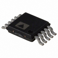
AD5324BRM Analog Devices Inc, AD5324BRM Datasheet - Page 19

AD5324BRM
Manufacturer Part Number
AD5324BRM
Description
Digital/Analog Converter IC Interface Type:Serial
Manufacturer
Analog Devices Inc
Datasheet
1.AD5304ARMZ-REEL7.pdf
(24 pages)
Specifications of AD5324BRM
Number Of Bits
12
Number Of Outputs
4
Package/case
10-SOIC
A/d, D/a Features
2.5 V To 5.5 V, 500 A Quad Voltage Output 12-Bit DAC
Mounting Type
Surface Mount
Rohs Status
RoHS non-compliant
Settling Time
6µs
Data Interface
Serial
Number Of Converters
4
Voltage Supply Source
Single Supply
Power Dissipation (max)
5mW
Operating Temperature
-40°C ~ 105°C
Package / Case
10-MSOP, Micro10™, 10-uMAX, 10-uSOP
Lead Free Status / RoHS Status
Available stocks
Company
Part Number
Manufacturer
Quantity
Price
Part Number:
AD5324BRMZ
Manufacturer:
ADI/亚德诺
Quantity:
20 000
Part Number:
AD5324BRMZ-REEL7
Manufacturer:
ADI/亚德诺
Quantity:
20 000
Opto-Isolated Interface for Process Control Applications
The AD5304/AD5314/AD5324 have a versatile 3-wire serial
inter-face, making them ideal for generating accurate voltages
in process control and industrial applications. Due to noise,
safety requirements, or distance, it might be necessary to iso-
late the AD5304/AD5314/AD5324 from the controller. This
can easily be achieved by using opto-isolators, which provide
isolation in excess of 3 kV. The actual data rate achieved is
limited by the type of opto-couplers chosen. The serial load-
ing structure of the AD5304/AD5314/AD5324 makes them
ideally suited for use in opto-isolated applications. Figure 42
shows an opto-isolated interface to the AD5304 where DIN,
SCLK, and SYNC are driven from opto-couplers. The power
supply to the part also needs to be isolated. This is done by
using a transformer. On the DAC side of the transformer, a
5 V regulator provides the 5 V supply required for the AD5304.
DECODING MULTIPLE AD5304/AD5314/AD5324S
The SYNC pin on the AD5304/AD5314/AD5324 can be used
in applications to decode a number of DACs. In this applica-
tion, all the DACs in the system receive the same serial clock
and serial data, but SYNC can only be active to one of the devices
at any one time, allowing access to four channels in this 16-channel
system. The 74HC139 is used as a 2-to-4-line decoder to address
any of the DACs in the system. To prevent timing errors, the
enable input must be brought to its inactive state while the
POWER
SYNC
SCLK
DIN
Figure 42. AD5304 in an Opto-Isolated Interface
10kΩ
10kΩ
10kΩ
REGULATOR
V
V
V
DD
DD
DD
5V
SCLK
SYNC
DIN
AD5304
V
GND
DD
V
V
V
V
REFIN
OUT
OUT
OUT
OUT
10µF
A
B
C
D
0.1µF
Rev. F | Page 19 of 24
coded address inputs are changing state. Figure 43 shows a
diagram of a typical setup for decoding multiple AD5304
devices in a system.
AD5304/AD5314/AD5324 as a Digitally Programmable
Window Detector
A digitally programmable upper/lower limit detector using two
DACs in the AD5304/AD5314/AD5324 is shown in Figure 44.
The upper and lower limits for the test are loaded to DAC A
and DAC B, which, in turn, set the limits on the CMP04. If the
signal at the V
an LED indicates the fail condition. Similarly, DAC C and DAC D
can be used for window detection on a second V
V
*ADDITIONAL PINS OMITTED FOR CLARITY.
REF
SYNC
SCLK
5V
ADDRESS
DIN
ENABLE
CODED
SCLK
DIN
Figure 43. Decoding Multiple AD5304 Devices in a System
0.1µF
REFIN
AD5304/AD5314/
SYNC
DIN
SCLK
AD5324*
IN
1G
1A
1B
input is not within the programmed window,
10µF
1/2
GND
74HC139
DGND
Figure 44. Window Detection
V
V
V
V
V
DD
CC
DD
OUT
OUT
AD5304/AD5314/AD5324
A
B
1Y0
1Y1
1Y2
1Y3
V
IN
CMP04
1/2
SYNC
DIN
SCLK
SYNC
DIN
SCLK
SYNC
DIN
SCLK
SYNC
DIN
SCLK
AD5304
AD5304
AD5304
AD5304
PASS/FAIL
1/6 74HC05
1kΩ
FAIL
IN
V
V
V
V
V
V
V
V
V
V
V
V
V
V
V
V
signal.
OUT
OUT
OUT
OUT
OUT
OUT
OUT
OUT
OUT
OUT
OUT
OUT
OUT
OUT
OUT
OUT
A
B
C
D
A
B
C
D
A
B
C
D
A
B
C
D
1kΩ
PASS


