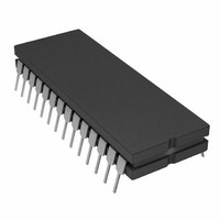
AD669SQ Analog Devices Inc, AD669SQ Datasheet - Page 2

AD669SQ
Manufacturer Part Number
AD669SQ
Description
IC,D/A CONVERTER,SINGLE,16-BIT,BICMOS,DIP,28PIN
Manufacturer
Analog Devices Inc
Series
DACPORT®r
Datasheet
1.AD669ANZ.pdf
(12 pages)
Specifications of AD669SQ
Rohs Status
RoHS non-compliant
Settling Time
10µs
Number Of Bits
16
Data Interface
Parallel
Number Of Converters
1
Voltage Supply Source
Dual ±
Power Dissipation (max)
625mW
Operating Temperature
-55°C ~ 125°C
Mounting Type
Through Hole
Package / Case
28-CDIP (0.600", 15.24mm)
Lead Free Status / RoHS Status
Available stocks
Company
Part Number
Manufacturer
Quantity
Price
AD669–SPECIFICATIONS
Model
RESOLUTION
DIGITAL INPUTS (T
TRANSFER FUNCTION CHARACTERISTICS
REFERENCE INPUT
REFERENCE OUTPUT
OUTPUT CHARACTERISTICS
POWER SUPPLIES
TEMPERATURE RANGE
NOTES
1
2
3
4
5
*Same as AD669AN/AR specification.
Specifications subject to change without notice.
Specifications in boldface are tested on all production units at final electrical test. Results from those tests are used to calculate outgoing quality levels. All min and max specifica-
tions are guaranteed. Those shown in boldface are tested on all production units.
For 16-bit resolution, 1 LSB = 0.0015% of FSR = 15 ppm of FSR. For 15-bit resolution, 1 LSB = 0.003% of FSR = 30 ppm of FSR. For 14-bit resolution
Gain error and gain drift measured using the internal reference. Gain drift is primarily reference related. See the Using the AD669 with the AD688 Reference section
External current is defined as the current available in addition to that supplied to REF IN and SPAN/BIPOLAR OFFSET on the AD669.
Operation on 12 V supplies is possible using an external reference like the AD586 and reducing the output range. Refer to the Internal/External Reference Use section.
Measured with fixed 50
1 LSB = 0.006% of FSR = 60 ppm of FSR. FSR stands for Full-Scale Range and is 10 V for a 0 V to + 10 V span and 20 V for a –10 V to +10 V span.
for further information.
the Analog Circuit Connections section.
V
V
I
I
Integral Nonlinearity
Differential Nonlinearity
Monotonicity Over Temperature
Gain Error
Gain Drift
Unipolar Offset
Unipolar Offset Drift (T
Bipolar Zero Error
Bipolar Zero Error Drift (T
Input Resistance
Bipolar Offset Input Resistance
Voltage
Drift
External Current
Capacitive Load
Short Circuit Current
Output Voltage Range
Output Current
Capacitive Load
Short Circuit Current
Voltage
Current (No Load)
Power Supply Sensitivity
Power Dissipation (Static, No Load)
Specified Performance (A, B)
Specified Performance (S)
IH
IL
IH
IL
T
T
Unipolar Configuration
Bipolar Configuration
V
V
V
I
I
I
(V
(V
CC
EE
LL
(Logic “0” )
(Logic “1” )
MIN
MIN
CC
EE
LL
@ V
@ V
IL
IH
4
4
= 0 V)
= 5.5 V)
to T
to T
IH
IH
2
2, 5
, V
, V
(T
MAX
MAX
IL
IL
MIN
= 5, 0 V
= 2.4, 0.4 V
3
to T
MIN
resistors. Eliminating these resistors increases the gain error by 0.25% of FSR (Unipolar mode) or 0.50% of FSR (Bipolar mode). Refer to
MAX
MIN
to T
)
MIN
to T
MAX
to T
MAX
)
MAX
)
)
1
(@ T
Min
16
2.0
0
14
7
7
9.98
2
0
–10
5
+13.5
–13.5
+4.5
–40
A
= +25 C, V
AD669AN/AR
Typ
10
10
10.00
4
25
25
+12
–12
0.3
3
1
365
–2–
CC
= +15 V, V
Max
5.5
0.8
25
5
12
13
13
10.02
25
1000
+10
+10
1000
+16.5
–16.5
+5.5
+18
–18
2
7.5
3
625
+85
10
10
2
4
2
4
0.15
5
15
Min
16
*
*
14
*
*
*
*
*
*
*
*
*
–40
–55
*
EE
AD669AQ/SQ
= –15 V, V
Typ
*
*
*
*
*
*
*
*
*
*
*
*
LL
*
*
*
*
*
*
*
*
15
3
10
15
*
*
*
*
*
*
*
+85
+125
Max
*
*
*
*
*
*
*
*
= +5 V, unless otherwise noted)
0.10
5
15
Min
16
*
*
15
*
*
*
*
*
*
*
*
*
*
–40
AD669BN/BQ/BR
Typ
*
*
*
*
*
*
*
*
*
*
*
*
Max
*
*
*
*
15
3
5
*
*
*
15
*
*
*
*
*
*
*
*
*
*
*
*
+85
1
2
1
2
0.10
2.5
10
Bits
Volts
Volts
LSB
LSB
LSB
LSB
Bits
% of FSR
ppm/ C
mV
ppm/ C
mV
ppm/ C
Volts
ppm/ C
mA
pF
mA
Volts
mA
pF
mA
Volts
Volts
Volts
mA
mA
mA
mA
ppm/%
mW
Units
k
k
Volts
C
C
REV. A
A
A


