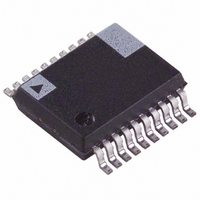
AD7226BRS-REEL Analog Devices Inc, AD7226BRS-REEL Datasheet - Page 2

AD7226BRS-REEL
Manufacturer Part Number
AD7226BRS-REEL
Description
Digital To Analog Converter
Manufacturer
Analog Devices Inc
Datasheet
1.AD7226KRZ.pdf
(16 pages)
Specifications of AD7226BRS-REEL
Rohs Status
RoHS non-compliant
Settling Time
4µs
Number Of Bits
8
Data Interface
Parallel
Number Of Converters
4
Voltage Supply Source
Dual ±
Operating Temperature
-40°C ~ 85°C
Mounting Type
Surface Mount
Package / Case
20-SSOP
Power Dissipation (max)
-
Lead Free Status / RoHS Status
AD7226–SPECIFICATIONS
DUAL SUPPLY
Parameter
STATIC PERFORMANCE
REFERENCE INPUT
DIGITAL INPUTS
DYNAMIC PERFORMANCE
POWER SUPPLIES
SWITCHING CHARACTERISTICS
NOTES
1
2
3
4
5
Specifications subject to change without notice.
Maximum possible reference voltage.
Temperature ranges are as follows:
Guaranteed by design. Not production tested.
Sample Tested at 25∞C to ensure compliance.
Switching Characteristics apply for single and dual supply operation.
Resolution
Total Unadjusted Error
Relative Accuracy
Differential Nonlinearity
Full-Scale Error
Full-Scale Temperature Coefficient
Zero Code Error
Zero Code Error Temperature Coefficient ± 50
Voltage Range
Input Resistance
Input Capacitance
Input High Voltage, V
Input Low Voltage, V
Input Leakage Current
Input Capacitance
Input Coding
Voltage Output Slew Rate
Voltage Output Settling Time
Digital Crosstalk
Minimum Load Resistance
V
I
I
Address to Write Setup Time, t
Address to Write Hold Time, t
Data Valid to Write Setup Time, t
Data Valid to Write Hold Time, t
Write Pulsewidth, t
DD
SS
DD
Range
K Version: –40∞C to +85∞C
B Version: –40∞C to +85∞C
3
WR
INL
INH
4
4
AH
AS
DH
DS
4, 5
K, B Versions
8
± 1
± 0.5
± 1
± 0.5
± 20
± 20
2 to (V
2
50
200
2.4
0.8
± 1
8
Binary
2.5
4
10
2
11.4/16.5
13
11
0
0
50
0
50
(V
unless otherwise noted. All Specifications T
DD
DD
– 4)
= 11.4 V to 16.5 V, V
2
–2–
Unit
Bits
LSB max
LSB max
LSB max
LSB max
ppm/∞C typ
mV max
mV/∞C typ
V min to V max
kW min
pF min
pF max
V min
V max
mA max
pF max
V/ms min
ms max
nV secs typ
kW min
V min/V max
mA max
mA max
ns min
ns min
ns min
ns min
ns min
SS
= –5 V
10%, AGND = DGND = 0 V; V
Conditions/Comments
V
Guaranteed Monotonic
V
Occurs when each DAC is loaded with all 0s.
Occurs when each DAC is loaded with all 1s.
V
V
V
For Specified Performance
Outputs Unloaded; V
Outputs Unloaded; V
MIN
DD
DD
IN
REF
OUT
to T
= 0 V or V
= 15 V ± 5%, V
= 14 V to 16.5 V, V
= 10 V; Settling Time to ± 1/2 LSB
= 10 V
MAX
unless otherwise noted.)
DD
REF
REF
IN
IN
= +2 V to (V
= V
= V
= 10 V
REF
INL
INL
= +10 V
or V
or V
DD
– 4 V)
REV.
INH
INH
1
,
D


