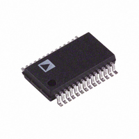
AD7714ARSZ-3 Analog Devices Inc, AD7714ARSZ-3 Datasheet - Page 15

AD7714ARSZ-3
Manufacturer Part Number
AD7714ARSZ-3
Description
28-BIT SIGMA DELTA A/D IC
Manufacturer
Analog Devices Inc
Datasheet
1.AD7714YNZ.pdf
(40 pages)
Specifications of AD7714ARSZ-3
Number Of Bits
24
Sampling Rate (per Second)
1k
Data Interface
DSP, MICROWIRE™, QSPI™, Serial, SPI™
Number Of Converters
1
Power Dissipation (max)
7mW
Voltage Supply Source
Analog and Digital
Operating Temperature
-40°C ~ 85°C
Mounting Type
Surface Mount
Package / Case
28-SSOP (0.200", 5.30mm Width)
Lead Free Status / RoHS Status
Lead free / RoHS Compliant
For Use With
EVAL-AD7714-3EBZ - BOARD EVALUATION FOR AD7714
Lead Free Status / RoHS Status
Lead free / RoHS Compliant
Available stocks
Company
Part Number
Manufacturer
Quantity
Price
Part Number:
AD7714ARSZ-3
Manufacturer:
ADI/亚德诺
Quantity:
20 000
CH2–CH0
Mode Register (RS2-RS0 = 0, 0, 1); Power On/Reset Status: 00 Hex
The Mode Register is an eight bit register from which data can either be read or to which data can be written. Table VIII outlines the
bit designations for the Mode Register.
REV. C
MD2
0
0
0
0
CH2
0
0
0
0
1
1
1
1
MD1
0
0
1
1
MD2
CH1
0
0
1
1
0
0
1
1
Channel Select. These three bits select a channel either for conversion or for access to calibration coefficients as
outlined in Table VII. There are three pairs of calibration registers on the part. In fully differential mode, the part
has three input channels so each channel has its own pair of calibration registers. In pseudo-differential mode, the
AD7714 has five input channels with some of the input channel combinations sharing calibration registers. With
CH2, CH1 and CH0 at a logic 1, the part looks at the AIN6 input internally shorted to itself. This can be used as
a test method to evaluate the noise performance of the part with no external noise sources. In this mode, the AIN6
input should be connected to an external voltage within the allowable common-mode range for the part. The
Power-On or RESET status of these bits is 1,0,0 selecting the differential pair AIN1 and AIN2.
MD0
0
1
0
1
mal conversions. This is the default condition of these bits after Power-On or RESET.
Communications Register. This is a one step calibration sequence and when complete the part returns to
Normal Mode with MD2, MD1 and MD0 returning to 0, 0, 0. The DRDY output or bit goes high when
calibration is initiated and returns low when this self-calibration is complete and a new valid word is
available in the data register. The zero-scale calibration is performed at the selected gain on internally
shorted (zeroed) inputs and the full-scale calibration is performed at the selected gain on an internally-
generated V
CH2, CH1 and CH0 of the Communications Register. Calibration is performed at the selected gain on
the input voltage provided at the analog input during this calibration sequence. This input voltage should
remain stable for the duration of the calibration. The DRDY output or bit goes high when calibration is
initiated and returns low when this zero-scale calibration is complete and a new valid word is available in
the data register. At the end of the calibration, the part returns to Normal Mode with MD2, MD1 and
MD0 returning to 0, 0, 0.
Calibration is performed at the selected gain on the input voltage provided at the analog input during this
calibration sequence. This input voltage should remain stable for the duration of the calibration. Once
again, the DRDY output or bit goes high when calibration is initiated and returns low when this full-scale
calibration is complete and a new valid word is available in the data register. At the end of the calibration,
the part returns to Normal Mode with MD2, MD1 and MD0 returning to 0, 0, 0.
Operating Mode
Normal Mode; this is the normal mode of operation of the device whereby the device is performing nor-
Self-Calibration; this activates self-calibration on the channel selected by CH2, CH1 and CH0 of the
Zero-Scale System Calibration; this activates zero scale system calibration on the channel selected by
Full-Scale System Calibration; this activates full-scale system calibration on the selected input channel.
CH0
0
1
0
1
0
1
0
1
MD1
REF
AIN1
AIN2
AIN3
AIN4
AIN1
AIN3
AIN5
AIN6
AIN(+)
/Selected Gain.
MD0
Table VII. Channel Selection
Table VIII. Mode Register
AIN6
AIN6
AIN6
AIN6
AIN2
AIN4
AIN6
AIN6
AIN(–)
G2
–15–
G1
Pseudo Differential
Pseudo Differential
Pseudo Differential
Pseudo Differential
Fully Differential
Fully Differential
Fully Differential
Test Mode
Type
G0
Calibration Register Pair
Register Pair 0
Register Pair 1
Register Pair 2
Register Pair 2
Register Pair 0
Register Pair 1
Register Pair 2
Register Pair 2
BO
FSYNC
AD7714
2


