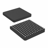
ADSP-2183KCAZ-210 Analog Devices Inc, ADSP-2183KCAZ-210 Datasheet - Page 25

ADSP-2183KCAZ-210
Manufacturer Part Number
ADSP-2183KCAZ-210
Description
16k16k16bit Dsp52 Mips3.3vmini Bgapbfree
Manufacturer
Analog Devices Inc
Series
ADSP-21xxr
Type
Fixed Pointr
Datasheet
1.ADSP-2183BSTZ-160.pdf
(31 pages)
Specifications of ADSP-2183KCAZ-210
Interface
Synchronous Serial Port (SSP)
Clock Rate
52MHz
Non-volatile Memory
External
On-chip Ram
80kB
Voltage - I/o
3.30V
Voltage - Core
3.30V
Operating Temperature
0°C ~ 70°C
Mounting Type
Surface Mount
Package / Case
144-MBGA, 144-Mini-BGA
Device Core Size
16b
Format
Fixed Point
Clock Freq (max)
52MHz
Mips
52
Device Input Clock Speed
52MHz
Ram Size
80KB
Operating Supply Voltage (typ)
3.3V
Operating Supply Voltage (min)
3V
Operating Supply Voltage (max)
3.6V
Operating Temp Range
0C to 70C
Operating Temperature Classification
Commercial
Mounting
Surface Mount
Pin Count
144
Package Type
CSPBGA
Package
144CSP-BGA
Numeric And Arithmetic Format
Fixed-Point
Maximum Speed
52 MHz
Device Million Instructions Per Second
52 MIPS
Lead Free Status / RoHS Status
Lead free / RoHS Compliant
Lead Free Status / RoHS Status
Lead free / RoHS Compliant
Available stocks
Company
Part Number
Manufacturer
Quantity
Price
Company:
Part Number:
ADSP-2183KCAZ-210
Manufacturer:
Analog Devices Inc
Quantity:
10 000
CAPACITIVE LOADING
Figures 22 and 23 show the capacitive loading characteristics of
the ADSP-2183.
TEST CONDITIONS
Output Disable Time
Output pins are considered to be disabled when they have
stopped driving and started a transition from the measured
output high or low voltage to a high impedance state. The out-
put disable time (t
as shown in the Output Enable/Disable diagram. The time is the
interval from when a reference signal reaches a high or low
voltage level to when the output voltages have changed by 0.5 V
from the measured output high or low voltage. The decay time,
t
load, i
lowing equation:
from which
DECAY
NOMINAL
L
, is dependent on the capacitive load, C
, on the output pin. It can be approximated by the fol-
25
20
15
10
18
16
14
12
10
–2
–4
–6
5
0
8
6
4
2
0
0
V
T = +85 C
DD
20
= 3.0V
DIS
t
40
DIS
40
) is the difference of t
t
DECAY
= t
60
MEASURED
80
80
=
C
C
100
C
L
L
L
– pF
– pF
• 0.5V
i
– t
L
120
120
DECAY
140
MEASURED
L
160
160
, and the current
180
and t
200
200
DECAY
,
is calculated. If multiple pins (such as the data bus) are dis-
abled, the measurement value is that of the last pin to stop
driving.
Output Enable Time
Output pins are considered to be enabled when they have made
a transition from a high-impedance state to when they start
driving. The output enable time (t
a reference signal reaches a high or low voltage level to when the
output has reached a specified high or low trip point, as shown
in the Output Enable/Disable diagram. If multiple pins (such as
the data bus) are enabled, the measurement value is that of the
first pin to start driving.
ENVIRONMENTAL CONDITIONS
Ambient Temperature Rating:
Package
LQFP
Mini-BGA
REFERENCE
T
T
PD = Power Dissipation in W
θ
θ
θ
OUTPUT
CA
JA
JC
(MEASURED)
AMB
CASE
(MEASURED)
OUTPUT
SIGNAL
= Thermal Resistance (Junction-to-Ambient)
= Thermal Resistance (Junction-to-Case)
= Thermal Resistance (Case-to-Ambient)
INPUT
= T
= Case Temperature in °C
OR
V
V
OUTPUT
OL
OH
CASE
OUTPUT STOPS
PIN
TO
t
t
MEASURED
DIS
DRIVING
– (PD × θ
50°C/W
70.7°C/W
1.5V
JA
50pF
V
V
HIGH-IMPEDANCE STATE. TEST CONDITIONS CAUSE
THIS VOLTAGE LEVEL TO BE APPROXIMATELY 1.5V.
OH
OL
t
DECAY
(MEASURED) +0.5V
(MEASURED) – 0.5V
CA
)
ENA
I
I
OH
OL
2°C/W
7.4°C/W
) is the interval from when
JC
ADSP-2183
OUTPUT STARTS
1.0V
2.0V
DRIVING
t
ENA
+1.5V
1.5V
V
(MEASURED)
V
(MEASURED)
OH
OL
48°C/W
63.3°C/W
CA


