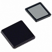
ADUC842BCPZ62-3 Analog Devices Inc, ADUC842BCPZ62-3 Datasheet - Page 8

ADUC842BCPZ62-3
Manufacturer Part Number
ADUC842BCPZ62-3
Description
Microconverter 1-cycle Version ADUC832
Manufacturer
Analog Devices Inc
Series
MicroConverter® ADuC8xxr
Specifications of ADUC842BCPZ62-3
Core Processor
8052
Core Size
8-Bit
Speed
8.38MHz
Connectivity
I²C, SPI, UART/USART
Peripherals
DMA, PSM, PWM, Temp Sensor, WDT
Number Of I /o
32
Program Memory Size
62KB (62K x 8)
Program Memory Type
FLASH
Ram Size
2.25K x 8
Voltage - Supply (vcc/vdd)
2.7 V ~ 3.6 V
Data Converters
A/D 8x12b, D/A 2x12b
Oscillator Type
Internal
Operating Temperature
-40°C ~ 85°C
Package / Case
56-LFCSP
Lead Free Status / RoHS Status
Lead free / RoHS Compliant
Eeprom Size
-
Lead Free Status / RoHS Status
Lead free / RoHS Compliant
ADuC841/ADuC842/ADuC843
ABSOLUTE MAXIMUM RATINGS
Table 2. T
Parameter
AV
AGND to DGND
DV
Digital Input Voltage to DGND
Digital Output Voltage to DGND
V
Analog Inputs to AGND
Operating Temperature Range,
Industrial
ADuC841BS,ADuC842BS,ADuC843BS
ADuC841BCP, ADuC842BCP,
ADuC843BCP
Storage Temperature Range
Junction Temperature
θ
θ
Lead Temperature, Soldering
ESD CAUTION
ESD (electrostatic discharge) sensitive device. Electrostatic charges as high as 4000 V readily accumulate on the
human body and test equipment and can discharge without detection. Although this product features
proprietary ESD protection circuitry, permanent damage may occur on devices subjected to high energy
electrostatic discharges. Therefore, proper ESD precautions are recommended to avoid performance
degradation or loss of functionality.
Vapor Phase (60 sec)
Infrared (15 sec)
JA
JA
REF
DD
DD
Thermal Impedance (ADuC84xBS)
Thermal Impedance (ADuC84xBCP)
to AGND
to DV
to DGND, AV
A
DD
= 25°C, unless otherwise noted
ADC0
ADC1
ADC6
ADC7
C
DD
REF
...
...
to AGND
SENSOR
TEMP
REFERENCE
BAND GAP
MUX
Figure 2. ADuC Block Diagram (Shaded Areas are Features Not Present on the ADuC812),
BUF
–0.3 V to +0.3 V
52°C/W
Rating
–0.3 V to +0.3 V
–0.3 V to +7 V
–0.3 V to DV
–0.3 V to DV
–0.3 V to AV
–0.3 V to AV
–40°C to +85°C
–65°C to +150°C
150°C
90°C/W
215°C
220°C
T/H
POR
No DACs on ADuC843, PLL on ADuC842/ADuC843 Only.
11-BIT STACK POINTER
2 kBYTES USER XRAM
62 kBYTES PROGRAM
FLASH/EE INCLUDING
2 × DATA POINTERS
USER DOWNLOAD
DD
DD
ASYNCHRONOUS
DD
DD
4 kBYTES DATA
ADuC841/ADuC842/ADuC843
SERIAL PORT
12-BIT
ADC
FLASH/EE
+ 0.3 V
+ 0.3 V
+ 0.3 V
+ 0.3 V
MODE
(UART)
DOWNLOADER
DEBUGGER
Rev. 0 | Page 8 of 88
CALIBRATION
CONTROL
ADC
AND
TIMER
UART
Stresses above those listed under Absolute Maximum Ratings
may cause permanent damage to the device. This is a stress
rating only and functional operation of the device at these or
any other conditions above those indicated in the operational
section of this specification is not implied. Exposure to absolute
maximum rating conditions for extended periods may affect
device reliability.
CORE
8052
MCU
CONTROL
SERIAL INTERFACE
DAC
SYNCHRONOUS
(I
256 BYTES USER
POWER SUPPLY
2
C AND SPI )
WATCHDOG
CONTROL
MONITOR
TIMER
PWM
RAM
OUTPUT DAC
OUTPUT DAC
TIME INTERVAL
(WAKE-UP CCT)
VOLTAGE
VOLTAGE
12-BIT
COUNTER
12-BIT
Σ -∆ DAC
Σ -∆ DAC
16-BIT
16-BIT
16-BIT
16-BIT
PWM
PWM
COUNTER
TIMERS
16-BIT
PLL
OSC
MUX
PWM1
DAC0
DAC1
PWM0
T0
T1
T2
T2EX
INT0
INT1


