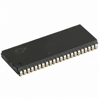
CY7C1021BNL-15VXCT Cypress Semiconductor Corp, CY7C1021BNL-15VXCT Datasheet

CY7C1021BNL-15VXCT
Specifications of CY7C1021BNL-15VXCT
Related parts for CY7C1021BNL-15VXCT
CY7C1021BNL-15VXCT Summary of contents
Page 1
... Note 1. For best practice recommendations, refer to the Cypress application note, Cypress Semiconductor Corporation Document #: 001-06494 Rev. *C CY7C1021BN, CY7C10211BN 1 Mbit (64K x 16) Static RAM Functional Description The CY7C1021BN/CY7C10211BN CMOS static RAM organized as 65,536 words by 16 bits. This device has an automatic power down feature that significantly reduces power consumption when deselected ...
Page 2
Contents Features ................................................................................1 Functional Description ........................................................1 Logic Block Diagram ...........................................................1 Contents ...............................................................................2 Selection Guide ...................................................................3 Pin Configuration ................................................................3 Pin Definitions ................................................................3 Maximum Ratings ................................................................4 Operating Range ..................................................................4 Electrical Characteristics ....................................................4 Capacitance .........................................................................5 Thermal Resistance .............................................................5 Document #: 001-06494 Rev. *C ...
Page 3
Selection Guide Description Maximum access time (ns) Maximum operating current (mA) Maximum CMOS standby current (mA) Commercial/Industrial Pin Configuration Pin Definitions Pin Name Pin Number A –A 1–5,18–21, 24–27, 42– I/O –I/O 7–10, 13–16, 29–32 35–38 ...
Page 4
Maximum Ratings Exceeding the maximum ratings may impair the useful life of the device. These user guidelines are not tested. Storage temperature ................................ –65 °C to +150 °C Ambient temperature with power applied ........................................... –55 °C to +125 °C [2] ...
Page 5
Capacitance [4] Parameter Description C Input capacitance IN C Output capacitance OUT Thermal Resistance [4] Parameter Description Θ Thermal resistance JA (junction to ambient) Θ Thermal resistance JC (junction to case) R 481Ω OUTPUT OUTPUT OUTPUT OUTPUT R2 ...
Page 6
Switching Characteristics [5] Over the operating range Parameter Description Read Cycle t Read cycle time RC t Address to data valid AA t Data hold from address change OHA t CE LOW to data valid ACE t OE LOW to ...
Page 7
Switching Waveforms ADDRESS DATA OUT PREVIOUS DATA VALID Figure 4. Read Cycle No. 2 (OE Controlled) ADDRESS CE t ACE OE t DOE BHE, BLE t LZOE t DBE t LZBE HIGH IMPEDANCE DATA OUT t LZCE ...
Page 8
Figure 5. Write Cycle No. 1 (CE Controlled) ADDRESS ADDRESS BHE, BLE DATA I/O Figure 6. Write Cycle No. 2 (BLE or BHE Controlled) ADDRESS t SA BHE, BLE WE CE DATA I/O Notes 12. Data ...
Page 9
Figure 7. Write Cycle No. 3 (WE Controlled, OE LOW) ADDRESS BHE, BLE DATA I/O Truth Table BLE BHE I High Data ...
Page 10
... Cypress maintains a worldwide network of offices, solution centers, manufacturers’ representatives and distributors. To find the office closest to you, visit us at http://www.cypress.com/go/datasheet/offices. Speed (ns) Ordering Code 12 CY7C1021BN-12ZXC 15 CY7C1021BNL-15VXC CY7C1021BN-15ZXC CY7C1021BN-15ZXI CY7C1021BNL-15ZXI CY7C1021BNL-15ZSXA CY7C1021BN-15VXE CY7C1021BN-15ZSXE Ordering Code Definition Technology: 250 nm Speed = ns; without ns Bus Width: x16 ...
Page 11
Package Diagrams Document #: 001-06494 Rev. *C CY7C1021BN, CY7C10211BN Figure 8. 44-Pin (400-Mil) Molded SOJ Figure 9. 44-Pin TSOP II 51-85082 *C 51-85087 *C Page [+] Feedback ...
Page 12
Acronyms Table 1. Acronyms Used in this Document Acronym Description BHE Byte high enable BLE Byte low enable CE Chip enable CMOS Complementary metal oxide semiconductor I/O Input/output OE Output enable SRAM Static random access memory TSOP Thin small outline ...
Page 13
... Corrected ‘Byte write select inputs’ to ‘Byte Enable select inputs’ on page 2. Ω Added ohm ( )symbol inThevenin equivalent circuit on page 4. Included T and T to Switching Characteristics table footnote 2 HZBE LZBE Included operating range for CY7C1021BNL-15ZXI in ordering information table. cypress.com/go/plc Revised June 11, 2010 CY7C1021BN, CY7C10211BN PSoC Solutions psoc.cypress.com/solutions PSoC 1 | PSoC 3 ...


