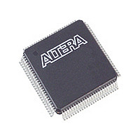
EPM570GT100I5N Altera, EPM570GT100I5N Datasheet - Page 37

EPM570GT100I5N
Manufacturer Part Number
EPM570GT100I5N
Description
MAX II
Manufacturer
Altera
Datasheet
1.EPM570GT100I5N.pdf
(88 pages)
Specifications of EPM570GT100I5N
Family Name
MAX II
Memory Type
Flash
# Macrocells
440
Frequency (max)
1.8797GHz
Propagation Delay Time
8.7ns
Number Of Logic Blocks/elements
57
# I/os (max)
76
Operating Supply Voltage (typ)
1.8V
In System Programmable
Yes
Operating Supply Voltage (min)
1.71V
Operating Supply Voltage (max)
1.89V
Operating Temp Range
-40C to 100C
Operating Temperature Classification
Industrial
Mounting
Surface Mount
Pin Count
100
Package Type
TQFP
Lead Free Status / Rohs Status
Compliant
Available stocks
Company
Part Number
Manufacturer
Quantity
Price
Company:
Part Number:
EPM570GT100I5N
Manufacturer:
ALTERA
Quantity:
52
Company:
Part Number:
EPM570GT100I5N
Manufacturer:
ALTERA
Quantity:
170
Chapter 2: MAX II Architecture
I/O Structure
Schmitt Trigger
Output Enable Signals
Programmable Drive Strength
© October 2008 Altera Corporation
1
Table 2–5. MAX II Devices and Speed Grades that Support 3.3-V PCI Electrical Specifications and
Meet PCI Timing
The input buffer for each MAX II device I/O pin has an optional Schmitt trigger
setting for the 3.3-V and 2.5-V standards. The Schmitt trigger allows input buffers to
respond to slow input edge rates with a fast output edge rate. Most importantly,
Schmitt triggers provide hysteresis on the input buffer, preventing slow-rising noisy
input signals from ringing or oscillating on the input signal driven into the logic array.
This provides system noise tolerance on MAX II inputs, but adds a small, nominal
input delay.
The JTAG input pins (TMS, TCK, and TDI) have Schmitt trigger buffers that are always
enabled.
The TCK input is susceptible to high pulse glitches when the input signal fall time is
greater than 200 ns for all I/O standards.
Each MAX II IOE output buffer supports output enable signals for tri-state control.
The output enable signal can originate from the GCLK[3..0] global signals or from
the MultiTrack interconnect. The MultiTrack interconnect routes output enable signals
and allows for a unique output enable for each output or bidirectional pin.
MAX II devices also provide a chip-wide output enable pin (DEV_OE) to control the
output enable for every output pin in the design. An option set before compilation in
the Quartus II software controls this pin. This chip-wide output enable uses its own
routing resources and does not use any of the four global resources. If this option is
turned on, all outputs on the chip operate normally when DEV_OE is asserted. When
the pin is deasserted, all outputs are tri-stated. If this option is turned off, the DEV_OE
pin is disabled when the device operates in user mode and is available as a user I/O
pin.
The output buffer for each MAX II device I/O pin has two levels of programmable
drive strength control for each of the LVTTL and LVCMOS I/O standards.
Programmable drive strength provides system noise reduction control for high
performance I/O designs. Although a separate slew-rate control feature exists, using
the lower drive strength setting provides signal slew-rate control to reduce system
noise and signal overshoot without the large delay adder associated with the
slew-rate control feature.
with drive strength control. The Quartus II software uses the maximum current
strength as the default setting. The PCI I/O standard is always set at 20 mA with no
alternate setting.
EPM1270
EPM2210
Device
Table 2–6
All Speed Grades
All Speed Grades
33-MHz PCI
shows the possible settings for the I/O standards
–3 Speed Grade
–3 Speed Grade
66-MHz PCI
MAX II Device Handbook
2–29


