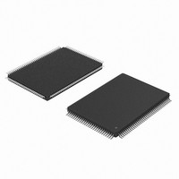
AD9862BST Analog Devices Inc, AD9862BST Datasheet - Page 19

AD9862BST
Manufacturer Part Number
AD9862BST
Description
IC FRONT-END MIXED-SGNL 128-LQFP
Manufacturer
Analog Devices Inc
Datasheet
1.AD9860-EBZ.pdf
(32 pages)
Specifications of AD9862BST
Rohs Status
RoHS non-compliant
Rf Type
LMDS, MMDS
Features
12-bit ADC(s), 14-bit DAC(s)
Package / Case
128-LQFP
Available stocks
Company
Part Number
Manufacturer
Quantity
Price
Company:
Part Number:
AD9862BSTZ
Manufacturer:
ADI
Quantity:
300
Part Number:
AD9862BSTZ
Manufacturer:
ADI/亚德诺
Quantity:
20 000
Interpolation Stage (Block C), Fine Modulation Stage (Block D),
Hilbert filter (Block E), and the Latch/Demultiplexing circuitry.
DAC
The DAC stage of the AD9860/AD9862 integrates a high perfor-
mance TxDAC core, a programmable gain control through a
Programmable Gain Amplifier (TxPGA), coarse gain control, and
offset adjustment and fine gain control to compensate for system
mismatches.
The TxDAC core of the AD9860/AD9862 provides dual, differen-
tial, complementary current outputs generated from the 12-/14-bit
data. The 12-/14-bit Dual DACs support update rates up to
128 MSPS. The differential outputs (i.e., IOUT+ and IOUT–)
of each dual DAC are complementary, meaning they always sum
to the full-scale current output of the DAC, I
ac performance is achieved with the differential current interface
drives balanced loads or a transformer.
The maximum full-scale output current, I
external resistor (R
The R
The relationship between I
Typically, R
optimal dynamic setting for the TxDACs. Increasing R
factor of 2 will proportionally decrease I
2. I
neously with the TxPGA Gain register or independently with
DAC A/B Coarse Gain registers.
The TxPGA function provides 20 dB of simultaneous gain
range for both DACs and is controlled by writing to SPI register
TxPGA Gain for a programmable full-scale output of 10% to
100% I
about 0.1 dB. Internally, the gain is controlled by changing the
main DAC bias currents with an internal TxPGA DAC whose
output is heavily filtered via an on-chip R-C filter to provide
continuous gain transitions. Note, the settling time and band-
width of the TxPGA DAC can be improved by a factor of 2 by
writing to the TxPGA Fast register.
Each DAC has independent coarse gain control. Coarse gain
control can be used to accommodate different I
dual DACs. The coarse full-scale output control can be adjusted
using the DAC A/B Coarse Gain registers to 1/2 or 1/11th of
the nominal full scale current.
REV. 0
OUTFSMAX
SET
OUTFSMAX
resistor is connected between the FSADJ Pin to ground.
SET
IOUT+A
IOUT–A
IOUT+B
IOUT–B
of each DAC can be re-scaled either simulta-
is 4 kW, which sets I
. The gain curve is linear in dB, with steps of
I
SET
OUTFSMAX
), which sets the DAC reference current.
PGA
PGA
BLOCK A
OUTFSMAX
DAC
~
TxDAC
TxDAC
67
¥
Ê
Á
Ë
OUTFSMAX
and R
1 23
R
.
OUTFSMAX
SET
QUADRATURE
BYPASSABLE
OUTFSMAX
V
SET
OUTFS
BLOCK B
Figure 3. Transmit Section Block Diagram
DIGITAL
MIXER
ˆ
˜
¯
f
f
S
to 20 mA, the
is:
S
/4,
/8
OUTFS
. Optimum
by a factor of
, is set by the
from the
INTERPOLATION
SET
BYPASSABLE
LOW-PASS
BLOCK C
FILTER
by a
–19–
QUADRATURE
BYPASSABLE
Fine Gain controls and dc offset controls can be used to compen-
sate for mismatches (for system level calibration), allowing improved
matching characteristics of the two Tx channels and aiding in suppres-
sing LO feedthrough. This is especially useful in image rejection
architectures. The 10-bit dc offset control of each DAC can be used
independently to provide a ± 12% I
differential pin, thus allowing calibration of any system offsets. The
fine gain control with 5-bit resolution allows the I
DAC to be varied over a ± 4% range, thus allowing compensation
of any DAC or system gain mismatches. Fine gain control is set
through the DAC A/B Fine Gain registers and the offset control
of each DAC is accomplished using DAC A/B Offset registers.
A power-down option allows the user to power down the analog
supply current to both DACs or either DAC, individually. A digital
power-down is also possible through either the Tx PwrDwn
register or the Mode/TxBlank pin.
Coarse Modulator
A digital coarse modulator is available in the transmit path to
shift the spectrum of the input data by ± f
input data consists of complex data, the modulator can be con-
figured to perform a complex modulation of the input spectrum.
If the data in the transmit path is not complex, a real mix can be
performed separately on each channel thereby frequency shifting
the real data and images by f
mixing is configured by setting the Real Mix register.
By default, the coarse modulator is bypassed. It can be configured
using Coarse Modulation and Neg Coarse Tune registers.
Interpolation Stage
Interpolation filters are available for use in the AD9860/AD9862
transmit path, providing 1 (bypassed), 2 , or 4 interpolation.
The interpolation filters effectively increase the Tx data rate while
suppressing the original images. The interpolation filters digitally
shift the worst case image further away from the desired signal,
thus reducing the requirements on the analog output reconstruc-
tion filter.
There are two 2 interpolation filters available in the Tx path.
An interpolation rate of 4 is achieved using both interpolation
filters; an interpolation rate of 2 is achieved by enabling only
the first 2
The first interpolation filter provides 2 interpolation using a
39 tap filter. It suppresses out-of-band signals by 60 dB or more
and has a flat passband response (less than 0.1 dB ripple) extend-
ing to 38% of the AD9860/AD9862 input Tx data rate (19% of
the DAC update rate, f
64 MSPS per channel when using 2 interpolation.
BLOCK D
DIGITAL
MIXER
DDS
I
Q
interpolation filter.
BLOCK E
HILBERT
HILBERT
FILTER
FILTER
DAC
). The maximum input data rate is
DAC
/4 or f
AD9860/AD9862
OUTFSMAX
DAC
DAC
/8. Real or complex
/4 or ± f
of offset to either
TxDATA
[0:13]
OUTFSMAX
DAC
/8. If the
of each


