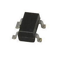
BF1211R NXP Semiconductors, BF1211R Datasheet

BF1211R
Specifications of BF1211R
Available stocks
Related parts for BF1211R
BF1211R Summary of contents
Page 1
... DATA SHEET BF1211; BF1211R; BF1211WR N-channel dual-gate MOS-FETs Product specification DISCRETE SEMICONDUCTORS 2003 Dec 16 ...
Page 2
... V digital and analog television tuner applications. DESCRIPTION Enhancement type N-channel field-effect transistor with source and substrate interconnected. Integrated diodes between gates and source protect against excessive input voltage surges. The BF1211, BF1211R and BF1211WR are encapsulated in the SOT143B, SOT143R and SOT343R plastic packages respectively. 3 handbook, 2 columns ...
Page 3
... THERMAL CHARACTERISTICS SYMBOL R thermal resistance from junction to soldering point th(j-s) BF1211; BF1211R BF1211WR 2003 Dec 16 BF1211; BF1211R; BF1211WR CAUTION PACKAGE DESCRIPTION plastic surface mounted package; 4 leads plastic surface mounted package; reverse pinning; 4 leads plastic surface mounted package; reverse pinning; 4 leads CONDITIONS ...
Page 4
... GG 2003 Dec 16 MDB828 (1) 150 200 T s (°C) CONDITIONS G1 G2-S DS note G2 G1 Product specification BF1211; BF1211R; BF1211WR MIN G1 G2 0.5 S- 0.5 S-G2 = 100 0 100 0. k G1-S G2-S MAX. UNIT 1 ...
Page 5
... L (opt 400 MHz mS mS (opt 800 MHz 3 (opt) input level for MHz; note 1 unw AGC AGC AGC 5 BF1211; BF1211R; BF1211WR MIN. TYP 2.1 1.1 0.9 15 3.5 S 0.9 1.3 (opt) ...
Page 6
... Gate 1 current as a function of gate 1 voltage; typical values. 2003 Dec 16 MDB829 handbook, halfpage (5) (6) (7) 1.5 2 2.5 V G1-S (V) ( G2-S MDB831 handbook, halfpage (1) (2) (3) (4) (5) (6) (7) 1 G1-S (V) ( G2-S 6 BF1211; BF1211R; BF1211WR (mA G2 1 1.2 V. G1-S G1-S ( 1 1.1 V. G1-S G1-S ( 1 G1-S G1-S Fig.6 Output characteristics ...
Page 7
... Dec 16 MDB833 handbook, halfpage (μA) MDB835 handbook, halfpage (1) (2) (3) (4) (5) (6) ( (V) ; see Fig.21 120 k BF1211; BF1211R; BF1211WR (mA G2 k (connected see Fig.21 Fig.10 Drain current as a function of gate 1 supply voltage (V ); typical values. GG ...
Page 8
... MDB837 handbook, halfpage reduction (1) (2) (3) (4) ( G2-S (V) ); see Fig.21 MDB839 handbook, halfpage gain reduction (dB C. amb 8 BF1211; BF1211R; BF1211WR 0 gain (dB) −10 −20 −30 −40 −50 − k (connected C. see Fig.21 MHz; T amb Fig.14 Typical gain reduction as a function of AGC voltage ...
Page 9
... mA Fig.18 Reverse transfer admittance and phase as MDB843 −10 2 handbook, halfpage ϕ (deg) (mS) −10 ϕ fs − (MHz mA Fig.20 Output admittance as a function of 9 Product specification BF1211; BF1211R; BF1211WR 3 10 ϕ (MHz C. amb a function of frequency; typical values −1 10 − (MHz ...
Page 10
... mA; T G2-S D amb F min (dB) (ratio) 0.9 0.693 1.3 0.707 10 Product specification BF1211; BF1211R; BF1211WR C3 4 ≈ 2.2 μH 50 Ω DUT C4 4 MGS315 = 25 C amb s 12 ANGLE MAGNITUDE (ratio) (deg) (ratio) 0.0005 89.3 0.993 ...
Page 11
... OUTLINE VERSION IEC SOT143B 2003 Dec scale 0.15 3.0 1.4 1.9 1.7 0.09 2.8 1.2 REFERENCES JEDEC JEITA 11 Product specification BF1211; BF1211R; BF1211WR detail 2.5 0.45 0.55 0.2 0.1 0.1 2.1 0.15 0.45 EUROPEAN PROJECTION SOT143B ISSUE DATE 04-11-16 06-03-16 ...
Page 12
... OUTLINE VERSION IEC SOT143R 2003 Dec scale 0.15 3.0 1.4 1.9 1.7 0.09 2.8 1.2 REFERENCES JEDEC JEITA SC-61AA 12 Product specification BF1211; BF1211R; BF1211WR detail 2.5 0.55 0.45 0.2 0.1 0.1 2.1 0.25 0.25 EUROPEAN PROJECTION SOT143R ISSUE DATE 04-11-16 06-03-16 ...
Page 13
... OUTLINE VERSION IEC SOT343R 2003 Dec scale 0.25 2.2 1.35 1.3 1.15 0.10 1.8 1.15 REFERENCES JEDEC EIAJ 13 BF1211; BF1211R; BF1211WR detail 2.2 0.45 0.23 0.2 0.2 2.0 0.15 0.13 EUROPEAN PROJECTION Product specification SOT343R 0.1 ISSUE DATE ...
Page 14
... Terms and conditions of commercial sale of NXP Semiconductors. 2003 Dec 16 BF1211; BF1211R; BF1211WR (2) This document contains data from the objective specification for product development. This document contains data from the preliminary specification. ...
Page 15
... Dec 16 BF1211; BF1211R; BF1211WR Export control This document as well as the item(s) described herein may be subject to export control regulations. Export might require a prior authorization from national authorities. Quick reference data ...
Page 16
... Interface, Security and Digital Processing expertise Customer notification This data sheet was changed to reflect the new company name NXP Semiconductors, including new legal definitions and disclaimers. No changes were made to the technical content, except for package outline drawings which were updated to the latest version. ...


