MMBD2835LT1G ON Semiconductor, MMBD2835LT1G Datasheet

DIODE SWITCH DUAL 35V SOT23

MMBD2835LT1G

Manufacturer Part Number
MMBD2835LT1G
Description
DIODE SWITCH DUAL 35V SOT23
Manufacturer
ON Semiconductor
Datasheet

Specifications of MMBD2835LT1G

Voltage - Forward (vf) (max) @ If
1.2V @ 100mA
Current - Reverse Leakage @ Vr
100nA @ 30V
Current - Average Rectified (io) (per Diode)
100mA (DC)
Voltage - Dc Reverse (vr) (max)
35V
Reverse Recovery Time (trr)
4ns
Diode Type
Standard
Speed
Small Signal =< 200mA (Io), Any Speed
Diode Configuration
1 Pair Common Anode
Mounting Type
Surface Mount
Package / Case
SOT-23-3, TO-236-3, Micro3™, SSD3, SST3
Lead Free Status / RoHS Status
Lead free / RoHS Compliant
Other names
MMBD2835LT1GOS
MMBD2835LT1GOS
MMBD2835LT1GOSTR

Available stocks

Company
Part Number
Manufacturer
Quantity
Price
Part Number:
MMBD2835LT1G
Manufacturer:
ON
Quantity:
6 000
Part Number:
MMBD2835LT1G
Manufacturer:
ON
Quantity:
30 000
Part Number:
MMBD2835LT1G
Manufacturer:
ON/安森美
Quantity:
20 000
MMBD2835LT1G,
MMBD2836LT1G
Monolithic Dual Switching
Diodes
Features
Stresses exceeding Maximum Ratings may damage the device. Maximum
Ratings are stress ratings only. Functional operation above the Recommended
Operating Conditions is not implied. Extended exposure to stresses above the
Recommended Operating Conditions may affect device reliability.
1. FR−5 = 1.0  0.75  0.062 in.
2. Alumina = 0.4  0.3  0.024 in. 99.5% alumina.
© Semiconductor Components Industries, LLC, 2009
August, 2009 − Rev. 5
MAXIMUM RATINGS (EACH DIODE)
THERMAL CHARACTERISTICS
Reverse Voltage
Forward Current
Total Device Dissipation FR− 5 Board
Thermal Resistance, Junction−to−Ambient
Total Device Dissipation Alumina
Thermal Resistance, Junction−to−Ambient
Junction and Storage Temperature
Compliant
These Devices are Pb−Free, Halogen Free/BFR Free and are RoHS
(Note 1)
T
Derate above 25°C
Substrate, (Note 2)
T
Derate above 25°C
A
A
= 25°C
= 25°C
Rating
MMBD2835LT1G
MMBD2836LT1G
Symbol
T
R
R
J
V
P
P
, T
I
qJA
qJA
F
R
D
D
stg
−55 to
Value
+150
100
225
556
300
417
1.8
2.4
35
75
1
mW/°C
mW/°C
mAdc
°C/W
°C/W
Unit
Vdc
mW
mW
°C
†For information on tape and reel specifications,
MMBD2835LT1G
MMBD2836LT1G
including part orientation and tape sizes, please
refer to our Tape and Reel Packaging Specifications
Brochure, BRD8011/D.
1
Device
*Date Code orientation and/or overbar may
vary depending upon manufacturing location.
xxx
M
G
(Note: Microdot may be in either location)
2
ORDERING INFORMATION
ANODE
MARKING DIAGRAM
3
3
= Specific Device Code
= Date Code
= Pb−Free Package
http://onsemi.com
1
A3X = MMBD2835LT1G
A2X = MMBD2836LT1G
(Pb−Free)
(Pb−Free)
Package
SOT−23
SOT−23
xxx MG
Publication Order Number:
SOT−23 (TO −236AB)
G
CASE 318 −08
STYLE 12
3000 / Tape & Reel
3000 / Tape & Reel
CATHODE
CATHODE
MMBD2835LT1/D
Shipping
1
2

Related parts for MMBD2835LT1G

MMBD2835LT1G Summary of contents

Page 1

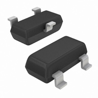
... CASE 318 −08 1 STYLE 12 2 MARKING DIAGRAM xxx xxx = Specific Device Code A3X = MMBD2835LT1G A2X = MMBD2836LT1G M = Date Code G = Pb−Free Package (Note: Microdot may be in either location) *Date Code orientation and/or overbar may vary depending upon manufacturing location. ORDERING INFORMATION Device ...

Page 2

... F 0.1 mF DUT 50 W OUTPUT PULSE GENERATOR Notes 2.0 kW variable resistor adjusted for a Forward Current (I Notes: 2. Input pulse is adjusted so I Notes 25°C unless otherwise noted) (EACH DIODE) A MMBD2835LT1G MMBD2836LT1G MMBD2835LT1G MMBD2836LT1G = 1.0 mAdc) (Figure 1) R(REC 0.1 mF 10% 90 INPUT SAMPLING V R OSCILLOSCOPE INPUT SIGNAL is equal ...

Page 3

CURVES APPLICABLE TO EACH CATHODE 100 T = 85° 1.0 0.1 0.2 0.4 0.6 0 FORWARD VOLTAGE (VOLTS) F Figure 2. Forward Voltage 1.75 1.50 1.25 1.00 0. -40°C A 1.0 ...

Page 4

... A A1 *For additional information on our Pb−Free strategy and soldering details, please download the ON Semiconductor Soldering and Mounting Techniques Reference Manual, SOLDERRM/D. ON Semiconductor and are registered trademarks of Semiconductor Components Industries, LLC (SCILLC). SCILLC reserves the right to make changes without further notice to any products herein. SCILLC makes no warranty, representation or guarantee regarding the suitability of its products for any particular purpose, nor does SCILLC assume any liability arising out of the application or use of any product or circuit, and specifically disclaims any and all liability, including without limitation special, consequential or incidental damages. “ ...

Related keywords