NDC7001C Fairchild Semiconductor, NDC7001C Datasheet
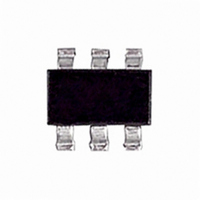
MOSFET N+P 60V 340MA SSOT6

NDC7001C

Manufacturer Part Number
NDC7001C
Description
MOSFET N+P 60V 340MA SSOT6
Manufacturer
Fairchild Semiconductor
Type
Power MOSFETr
Datasheet

Specifications of NDC7001C

Fet Type
N and P-Channel
Fet Feature
Logic Level Gate
Rds On (max) @ Id, Vgs
2 Ohm @ 510mA, 10V
Drain To Source Voltage (vdss)
60V
Current - Continuous Drain (id) @ 25° C
510mA, 340mA
Vgs(th) (max) @ Id
2.5V @ 250µA
Gate Charge (qg) @ Vgs
1.5nC @ 10V
Input Capacitance (ciss) @ Vds
20pF @ 25V
Power - Max
700mW
Mounting Type
Surface Mount
Package / Case
6-SSOT, SuperSOT-6
Number Of Elements
2
Polarity
N/P
Channel Mode
Enhancement
Drain-source On-volt
60V
Gate-source Voltage (max)
±20V
Power Dissipation
960mW
Output Power (max)
Not RequiredW
Frequency (max)
Not RequiredMHz
Noise Figure
Not RequireddB
Power Gain
Not RequireddB
Drain Efficiency
Not Required%
Operating Temp Range
-55C to 150C
Operating Temperature Classification
Military
Mounting
Surface Mount
Pin Count
6
Package Type
SuperSOT
Configuration
Dual
Transistor Polarity
N and P-Channel
Resistance Drain-source Rds (on)
2 Ohm @ 10 V @ N Channel
Drain-source Breakdown Voltage
60 V
Gate-source Breakdown Voltage
+/- 20 V
Continuous Drain Current
0.51 A @ N Channel or 0.34 A @ P Channel
Maximum Operating Temperature
+ 150 C
Mounting Style
SMD/SMT
Minimum Operating Temperature
- 55 C
Continuous Drain Current Id
340mA
Drain Source Voltage Vds
50V
On Resistance Rds(on)
7.5ohm
Rds(on) Test Voltage Vgs
10V
Threshold Voltage Vgs Typ
2.1V
Rohs Compliant
Yes
Lead Free Status / RoHS Status
Lead free / RoHS Compliant
Other names
NDC7001CTR

Available stocks

Company
Part Number
Manufacturer
Quantity
Price
Part Number:
NDC7001C
Manufacturer:
FSC
Quantity:
36 000
Part Number:
NDC7001C
Manufacturer:
FSC
Quantity:
24 000
Part Number:
NDC7001C
Manufacturer:
FAIRCHILD/仙童
Quantity:
20 000
Part Number:
NDC7001C
0
Company:
Part Number:
NDC7001C
Quantity:
16 754
Part Number:
NDC7001C-NL
Manufacturer:
FAIRCHILD/仙童
Quantity:
20 000
NDC7001C
Dual N & P-Channel Enhancement Mode Field Effect Transistor
General Description
These dual N & P-Channel Enhancement Mode Field
Effect Transistors are produced using Fairchild’s
proprietary, high cell density, DMOS technology. This
very high density process has been designed to
minimize on-state resistance, provide rugged and
reliable performance and fast switching. These
device is particularly suited for low voltage, low
current, switching, and power supply applications.
2002 Fairchild Semiconductor Corporation
Absolute Maximum Ratings
Symbol
V
V
I
P
T
Thermal Characteristics
R
R
Package Marking and Ordering Information
D
J
DSS
GSS
D
, T
JA
JC
Device Marking
STG
SuperSOT
.01C
Drain-Source Voltage
Gate-Source Voltage
Drain Current
Power Dissipation for Single Operation
Operating and Storage Junction Temperature Range
Thermal Resistance, Junction-to-Ambient
Thermal Resistance, Junction-to-Case
D1
S1
TM
-6
D2
– Continuous
– Pulsed
NDC7001C
Device
G1
Parameter
S2
G2
T
A
=25
o
C unless otherwise noted
Reel Size
7’’
Features
(Note 1a)
(Note 1a)
(Note 1b)
(Note 1a)
(Note 1c)
(Note 1)
Q1
Q2 –0.34 A, 60V.
High saturation current
High density cell design for low R
Proprietary SuperSOT
lead frame for superior thermal and electrical capabilities
0.51 A, 60V.
0.51
4
5
6
Q1
1.5
60
20
Tape width
–55 to +150
TM
8mm
R
R
R
R
–6 package: design using copper
DS(ON)
DS(ON)
DS(ON)
DS(ON)
0.96
130
0.9
0.7
60
= 2
= 4
= 5
= 7.5
Q2(P)
Q1(N)
DS(ON)
–0.34
Q2
–60
–1
20
@ V
@ V
@ V
@ V
3
2
1
GS
GS
GS
May 2002
NDC7001C Rev B (W)
GS
= 10 V
= 4.5 V
= –10 V
Quantity
= –4.5 V
3000
Units
C/W
W
V
A
C

Related parts for NDC7001C

NDC7001C Summary of contents

Page 1

... Reel Size 7’’ May 2002 DS(ON 4.5 V DS(ON –10 V DS(ON 7 –4.5 V DS(ON) GS DS(ON) TM –6 package: design using copper Q2( Q1( Units 60 – 0.51 –0.34 A 1.5 –1 0.96 0.9 W 0.7 –55 to +150 C C/W 130 60 Tape width Quantity 8mm 3000 NDC7001C Rev B (W) ...

Page 2

... V –60 67 mV/ C – –1 100 nA –100 nA 1 2.1 2.5 V –1 –1.9 –3.5 mV/ C –3.8 3 1.7 3.5 1.2 5 1.5 7.5 1.9 10 1.5 A –1 380 mS 700 4 11.2 11.2 2.8 5.6 ns 3.2 6 1.1 1.5 nC 1.6 2.2 0.2 nC 0.3 0.4 nC 0.3 NDC7001C Rev B (W) ...

Page 3

... A/µ –0. 100 A/µ 0. 100 A/µ –0. 100 A/µ determined by the user's board design 140°C/W when mounted .005 in pad copper Min Typ Max Units 0. –0.34 Q2 0.8 1.2 V –0.8 –1 180°C/W when mounted on a minimum pad. NDC7001C Rev B (W) ...

Page 4

... Figure 6. Body Diode Forward Voltage Variation with Source Current and Temperature. 5.0V 6.0V 7.0V 8.0V 10V 0.3 0.6 0.9 1 DRAIN CURRENT ( 0.26A 125 GATE TO SOURCE VOLTAGE (V) GS Gate-to-Source Voltage 125 -55 C 0.4 0.6 0 BODY DIODE FORWARD VOLTAGE (V) SD NDC7001C Rev B (W) 1.5 10 1.2 ...

Page 5

... Figure 10. Single Pulse Maximum 0.01 0 TIME (sec 1MHz ISS C OSS DRAIN TO SOURCE VOLTAGE (V) DS SINGLE PULSE R = 180°C 25°C A 0.01 0 TIME (sec) 1 Power Dissipation. R ( 180 °C/W JA P(pk ( Duty Cycle 100 NDC7001C Rev B (W) 60 100 1000 ...

Page 6

... Figure 16. Body Diode Forward Voltage Variation with Source Current and Temperature. -3.5V -4.0V -4.5V -6.0V -10V 0.2 0.4 0.6 0 DRAIN CURRENT ( -0.17A 125 GATE TO SOURCE VOLTAGE (V) GS Gate-to-Source Voltage 125 -55 C 0.4 0.6 0 BODY DIODE FORWARD VOLTAGE (V) SD NDC7001C Rev B ( 1.2 ...

Page 7

... Figure 20. Single Pulse Maximum 0.01 0 TIME (sec MHz ISS C OSS DRAIN TO SOURCE VOLTAGE (V) DS SINGLE PULSE R = 180°C 25° 100 t , TIME (sec) 1 Power Dissipation. R ( 180 °C/W JA P(pk ( Duty Cycle 100 1000 NDC7001C Rev B (W) ...

Page 8

CROSSVOLT â â â â Rev. H5 ...

Related keywords