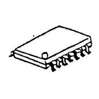
NJU8714VB2-TE2 NJR, NJU8714VB2-TE2 Datasheet

NJU8714VB2-TE2
Specifications of NJU8714VB2-TE2
Related parts for NJU8714VB2-TE2
NJU8714VB2-TE2 Summary of contents
Page 1
... SEL BEEP IN Ver.2004-05-21 FOR Class D AMPLIFIER selects “Synchronous” or HALTB BEEP : 0V to 2.0V OUT V G Level Shifter Control Logic Level Shifter Control Logic Level Shifter Level Shifter Level Shifter Level Shifter PACKAGE OUTLINE NJU8714VB2 PIN CONFIGURATION MCK IN1 BEEP1 OUT SSO 9 ...
Page 2
NJU8714 TERMINAL DESCRIPTION No. SYMBOL 1 MCK HALTB 4 D IN1 5 BEEP BEEP1 7 OUT 1 8,13 V SSO 9 OUT DDO1 11 V DDO2 12 OUT 2X 14 ...
Page 3
FUNCTIONAL DESCRIPTION (1) Signal Output The OUT and OUT 1/1X 2/2X converted to analog signals via external 2nd-order or higher LC filter. A switching regulator with a high response against a voltage fluctuation is the best selection for the V ...
Page 4
NJU8714 ABSOLUTE MAXIMUM RATINGS PARAMETER Supply Voltage Input Voltage Operating Temperature Storage Temperature Power Dissipation Note.1) All voltage values are specified as V Note.2) If the LSI is used on condition beyond the absolute maximum rating, the LSI may be ...
Page 5
TIMING CHARACTERISTICS Audio Signal Input MCK D ,D IN1 IN2 (Ta= =2.5V PARAMETER MCK Frequency MCK Pulse Width (H) MCK Pulse Width ( Setup Time IN1 IN2 D ,D Hold Time IN1 IN2 BEEP ...
Page 6
NJU8714 APPLICATION CIRCUIT -Load Impedance: 32Ω MCK(1) HALTB(3) STBYB(18) SEL(19 10uF 2. -Load Impedance: 8Ω MCK(1) HALTB(3) STBYB(18) SEL(19 10uF 2. Note 3) De-coupling capacitors must ...
Page 7
Ver.2004-05-21 NJU8714 NJU3555 NJU3555 [CAUTION] The specifications on this databook are only given for information , without any guarantee as regards either mistakes or omissions. The application circuits in this databook are described only to show representative usages of the ...


