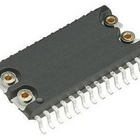
M41T94MH6 STMicroelectronics, M41T94MH6 Datasheet - Page 17

M41T94MH6
Manufacturer Part Number
M41T94MH6
Description
Real Time Clock Serial 512 (64x8)
Manufacturer
STMicroelectronics
Datasheet
1.M41T94MQ6TR.pdf
(41 pages)
Specifications of M41T94MH6
Function
Clock, Calendar, Alarm, Timer Interrupt
Rtc Memory Size
64 B
Supply Voltage (max)
5.5 V
Supply Voltage (min)
2.7 V
Maximum Operating Temperature
+ 85 C
Minimum Operating Temperature
- 40 C
Mounting Style
SMD/SMT
Rtc Bus Interface
Serial
Package / Case
SO-28
Time Format
HH:MM:SS:hh
Lead Free Status / RoHS Status
Lead free / RoHS Compliant
Available stocks
Company
Part Number
Manufacturer
Quantity
Price
Company:
Part Number:
M41T94MH6E
Manufacturer:
ST
Quantity:
740
Company:
Part Number:
M41T94MH6F
Manufacturer:
AOS
Quantity:
26 700
Part Number:
M41T94MH6F
Manufacturer:
ST
Quantity:
20 000
Company:
Part Number:
M41T94MH6TR
Manufacturer:
AD
Quantity:
6 230
M41T94
4
4.1
4.2
Clock operations
The eight byte clock register (see
read the date and time from the clock, in a binary coded decimal format. Tenths/hundredths
of seconds, seconds, minutes, and hours are contained within the first four registers. Bits D6
and D7 of clock register 03h (century/hours register) contain the CENTURY ENABLE bit
(CEB) and the CENTURY bit (CB). Setting CEB to a '1' will cause CB to toggle, either from
'0' to '1' or from '1' to '0' at the turn of the century (depending upon its initial state). If CEB is
set to a '0,' CB will not toggle. Bits D0 through D2 of register 04h contain the day (day of
week). Registers 05h, 06h, and 07h contain the date (day of month), month and years. The
ninth clock register is the control register (this is described in the clock calibration section).
Bit D7 of register 01h contains the STOP bit (ST). Setting this bit to a '1' will cause the
oscillator to stop. If the device is expected to spend a significant amount of time on the shelf,
the oscillator may be stopped to reduce current drain. When reset to a '0' the oscillator
restarts within one second.
The eight clock registers may be read one byte at a time, or in a sequential block. The
control register (address location 08h) may be accessed independently. Provision has been
made to assure that a clock update does not occur while any of the eight clock addresses
are being read. If a clock address is being read, an update of the clock registers will be
halted. This will prevent a transition of data during the READ.
Power-down time-stamp
When a power failure occurs, the halt update bit (HT) will automatically be set to a '1.' This
will prevent the clock from updating the clock registers, and will allow the user to read the
exact time of the power-down event. Resetting the HT bit to a '0' will allow the clock to
update the clock registers with the current time. For more information, see application note
AN1572.
Clock registers
The M41T94 offers 20 internal registers which contain clock, alarm, watchdog, flag, square
wave and control data (see
which contain external (user accessible) and internal copies of the data (usually referred to
as BiPORT
they are updated periodically by the simultaneous transfer of the incremented internal copy.
The internal divider (or clock) chain will be reset upon the completion of a WRITE to any
clock address.
The system-to-user transfer of clock data will be halted whenever the clock addresses (00h
to 07h) are being written. The update will resume either due to a deselect condition or when
the pointer increments to a non-clock or RAM address.
Clock and alarm registers store data in BCD. Control, watchdog and square wave registers
store data in binary format.
™
cells). The external copies are independent of internal functions except that
Table 4 on page
Table 4 on page
18). These registers are memory locations
18) is used to both set the clock and to
Clock operations
17/41


