NDB6060L Fairchild Semiconductor, NDB6060L Datasheet

MOSFET N-CH 60V 48A TO-263AB

NDB6060L

Manufacturer Part Number
NDB6060L
Description
MOSFET N-CH 60V 48A TO-263AB
Manufacturer
Fairchild Semiconductor
Type
Power MOSFETr
Datasheet

Specifications of NDB6060L

Fet Type
MOSFET N-Channel, Metal Oxide
Fet Feature
Logic Level Gate
Rds On (max) @ Id, Vgs
20 mOhm @ 24A, 10V
Drain To Source Voltage (vdss)
60V
Current - Continuous Drain (id) @ 25° C
48A
Vgs(th) (max) @ Id
2V @ 250µA
Gate Charge (qg) @ Vgs
60nC @ 5V
Input Capacitance (ciss) @ Vds
2000pF @ 25V
Power - Max
100W
Mounting Type
Surface Mount
Package / Case
D²Pak, TO-263 (2 leads + tab)
Configuration
Single
Transistor Polarity
N-Channel
Resistance Drain-source Rds (on)
0.02 Ohm @ 10 V
Drain-source Breakdown Voltage
60 V
Gate-source Breakdown Voltage
+/- 16 V
Continuous Drain Current
48 A
Power Dissipation
100000 mW
Maximum Operating Temperature
+ 175 C
Mounting Style
SMD/SMT
Minimum Operating Temperature
- 65 C
Number Of Elements
1
Polarity
N
Channel Mode
Enhancement
Drain-source On-res
0.02Ohm
Drain-source On-volt
60V
Gate-source Voltage (max)
±16V
Operating Temp Range
-65C to 175C
Operating Temperature Classification
Military
Mounting
Surface Mount
Pin Count
2 +Tab
Package Type
D2PAK
Lead Free Status / RoHS Status
Lead free / RoHS Compliant
Other names
NDB6060LTR

Available stocks

Company
Part Number
Manufacturer
Quantity
Price
Part Number:
NDB6060L
Manufacturer:
FSC
Quantity:
5 600
Absolute Maximum Ratings
________________________________________________________________________________
© 1997 Fairchild Semiconductor Corporation
Symbol
V
V
V
I
P
T
T
D
NDP6060L / NDB6060L
N-Channel Logic Level Enhancement Mode Field Effect Transistor
DSS
DGR
GSS
D
J
L
These logic level N-Channel enhancement mode power
field effect transistors are produced using Fairchild's
proprietary, high cell density, DMOS technology. This
very high density process has been especially tailored to
minimize on-state resistance, provide superior switching
performance, and withstand high energy pulses in the
avalanche and commutation modes. These devices are
particularly suited for low voltage applications such as
automotive, DC/DC converters, PWM motor controls,
and other battery powered circuits where fast switching,
low in-line power loss, and resistance to transients are
needed.
General Description
,T
STG
Parameter
Drain-Source Voltage
Drain-Gate Voltage (R
Gate-Source Voltage - Continuous
Drain Current
Total Power Dissipation @ T
Operating and Storage Temperature
Maximum lead temperature for soldering
purposes, 1/8" from case for 5 seconds
- Nonrepetitive (t
Derate above 25°C
- Continuous
- Pulsed
GS
< 1 M )
C
P
= 25°C
< 50 µs)
T
C
= 25°C unless otherwise noted
NDP6060L
Features
48A, 60V. R
Low drive requirements allowing operation directly from logic
drivers. V
Critical DC electrical parameters specified at elevated
temperature.
Rugged internal source-drain diode can eliminate the need
for an external Zener diode transient suppressor.
175°C maximum junction temperature rating.
High density cell design for extremely low R
TO-220 and TO-263 (D
and surface mount applications.
GS(TH)
DS(ON)
-65 to 175
< 2.0V.
± 16
± 25
0.67
144
100
275
60
60
48
= 0.025
2
PAK) package for both through hole
@ V
NDB6060L
G
GS
= 5V.
NDP6060L Rev. D / NDB6060L Rev. E
D
DS(ON)
S
.
April 1996
Units
W/°C
°C
°C
W
V
V
V
A

Related parts for NDB6060L

NDB6060L Summary of contents

Page 1

... C NDP6060L < 50 µ 25°C = 0.025 @ V = 5V. DS(ON) GS < 2.0V. GS(TH) . DS(ON) 2 PAK) package for both through hole NDB6060L 60 60 ± 16 ± 144 100 0.67 -65 to 175 275 NDP6060L Rev NDB6060L Rev. E April 1996 Units W/°C °C °C ...

Page 2

... MHz GEN Min Typ Max 200 48 60 250 125°C J 100 -100 125°C 0.65 1.5 J 0.025 0. 125° 1630 2000 460 800 150 400 15 30 320 500 49 100 161 300 36 60 8.2 21 NDP6060L Rev NDB6060L Rev. E Units µ ...

Page 3

... Thermal Resistance, Junction-to-Case R JC Thermal Resistance, Junction-to-Ambient R JA Note: 1. Pulse Test: Pulse Width < 300 µs, Duty Cycle < 2.0%. Conditions (Note 125° /dt = 100 A/µs F Min Typ Max Units 48 A 144 A 1 140 1.5 °C/W 62.5 °C/W NDP6060L Rev NDB6060L Rev. E ...

Page 4

... Figure 6. Gate Threshold Variation with V = 3.0V GS 3.5 4.0 4.5 5 DRAIN CURRENT (A) D Voltage and Drain Current 5. 125°C J 25°C -55° DRAIN CURRENT (A) D Current and Temperature 250µ 100 125 T , JUNCTION TEMPERATURE (°C) J Temperature. NDP6060L Rev NDB6060L Rev. E 5.5 6 100 = V GS 150 175 ...

Page 5

... Figure 10. Gate Charge Characteristics t d(on 125°C J 25°C -55° 0.4 0.6 0.8 1 1.2 1 BODY DIODE FORWARD VOLTAGE (V) SD Variation with Current and Temperature V = 12V = 48A DS D 48V 24V GATE CHARGE (nC d(off PULSE W IDTH Figure 12. Switching Waveforms. NDP6060L Rev NDB6060L Rev 1.6 1 INVERTED ...

Page 6

... Figure 15. Transient Thermal Response Curve. (continued SINGLE PULSE 1.5 C 25° =10V Figure 14. Maximum Safe Operating. Area 0 ,TIME ( DRAIN-SOURCE VOLTAGE ( ( 1.5 °C/W JC P(pk ( Duty Cycle 100 200 500 NDP6060L Rev NDB6060L Rev. E 1000 ...

Page 7

... These larger or intermediate boxes then will b e placed finally inside a labeled shipping box whic h still comes in different sizes depending on the number of units shipped. FSCINT Labe l samp le FAIRCHILD SEMICONDUCTOR CORPORATION HTB:B CBVK741B019 1080 LOT: ...

Page 8

TO-220 Tape and Reel Data and Package Dimensions, continued TO-220 (FS PKG Code 37) 1:1 Scale 1:1 on letter size paper Dimensions shown below are in: inches [millimeters] Part Weight per unit (gram): 1.4378 September 1998, Rev. A ...

Page 9

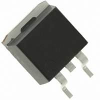
TO-263AB/D 2 PAK Tape and Reel Data and Package Dimensions 2 TO-263AB/D PAK Packaging Configuration: Figure 1.0 Customized Label 2 TO-263AB/D PAK Packaging Information Standard L86Z Packaging Option (no flow code) Packaging type TNR Rail/Tube Qty per Reel/Tube/Bag 800 45 ...

Page 10

TO-263AB/D 2 PAK Tape and Reel Data and Package Dimensions, continued 2 TO-263AB/D PAK Embossed Carrier Tape Configuration: Figure 3 Pkg type O263AB/ 10.60 15.80 24.0 1. PAK +/-0.10 ...

Page 11

TO-263AB/D 2 PAK Tape and Reel Data and Package Dimensions, continued TO-263AB/D 2 PAK (FS PKG Code 45) Scale 1:1 on letter size paper Dimensions shown below are in: Part Weight per unit (gram): 1.4378 1:1 inches [millimeters] August 1998, ...

Page 12

... TRADEMARKS The following are registered and unregistered trademarks Fairchild Semiconductor owns or is authorized to use and is not intended exhaustive list of all such trademarks. ACEx™ CoolFET™ CROSSVOLT™ CMOS FACT™ FACT Quiet Series™ ® FAST FASTr™ GTO™ ...

Related keywords