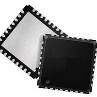
LAN88710_samples SMSC, LAN88710_samples Datasheet - Page 77

LAN88710_samples
Manufacturer Part Number
LAN88710_samples
Description
Ethernet ICs MII/RMII 10/100 Automot Transceiver
Manufacturer
SMSC
Datasheet
1.LAN88710BM_SAMPLES.pdf
(80 pages)
Specifications of LAN88710_samples
Ethernet Connection Type
10BASE-T, 100BASE-TX
Minimum Operating Temperature
- 40 C
Mounting Style
SMD/SMT
Product
Ethernet Transceivers
Standard Supported
IEEE802.3, IEEE802.3u
Supply Voltage (max)
3.6 V
Supply Voltage (min)
1.6 V
Maximum Operating Temperature
+ 85 C
Package / Case
QFN-32
Lead Free Status / RoHS Status
Lead free / RoHS Compliant
Small Footprint MII/RMII 10/100 Ethernet Transceiver for Automotive Applications
Datasheet
SMSC LAN88710AM/LAN88710BM
5.7
Crystal Cut
Crystal Oscillation Mode
Crystal Calibration Mode
Frequency
Frequency Tolerance at 25
Frequency Stability Over Temp
Frequency Deviation Over Time
Total Allowable PPM Budget
Shunt Capacitance
Load Capacitance
Drive Level
Equivalent Series Resistance
Operating Temperature Range
XTAL1/CLKIN Pin Capacitance
XTAL2 Pin Capacitance
PARAMETER
The device can accept either a 25 MHz crystal or a 25 MHz single-ended clock oscillator (±50 ppm)
input. If the single-ended clock oscillator method is implemented, XTAL2 should be left unconnected
and XTAL1/CLKIN should be driven with a nominal 0 - 3.3 V clock signal. See
recommended crystal specifications.
Note 5.20 The maximum allowable values for frequency tolerance and frequency stability are
Note 5.21 Frequency Deviation Over Time is also referred to as Aging.
Note 5.22 The total deviation for the Transmitter Clock Frequency is specified by IEEE 802.3u as
Note 5.23 +85
Note 5.24 This number includes the pad, the bond wire and the lead frame. PCB capacitance is not
Clock Circuit
application dependant. Since any particular application must meet the IEEE ±50 ppm Total
PPM Budget, the combination of these two values must be approximately ±45 ppm
(allowing for aging).
±100 ppm.
included in this value. The XTAL1/CLKIN pin, XTAL2 pin and PCB capacitance values are
required to accurately calculate the value of the two external load capacitors. The total load
capacitance must be equivalent to what the crystal expects to see in the circuit so that the
crystal oscillator will operate at 25.000 MHz.
o
C
o
C for grade A temperature range, +105
SYMBOL
F
F
F
F
P
Table 5.14 Crystal Specifications
C
temp
C
R
fund
age
tol
W
O
L
1
DATASHEET
MIN
300
-40
Parallel Resonant Mode
-
-
-
-
-
-
-
-
-
-
77
Fundamental Mode
AT, typ
±3 to 5
25.000
20 typ
NOM
7 typ
3 typ
3 typ
-
-
-
-
-
-
o
C for grade B temperature range
Note 5.23
MAX
±50
±50
±50
30
-
-
-
-
-
-
-
UNITS
MHz
ppm
ppm
ppm
ppm
µW
Revision 1.1 (05-26-10)
pF
pF
o
pF
pF
Ω
C
Table 5.14
Note 5.20
Note 5.20
Note 5.21
Note 5.22
Note 5.24
Note 5.24
NOTES
for the


