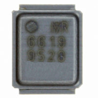
IRF6619TR1 International Rectifier, IRF6619TR1 Datasheet - Page 6

IRF6619TR1
Manufacturer Part Number
IRF6619TR1
Description
MOSFET N-CH 20V 30A DIRECTFET
Manufacturer
International Rectifier
Series
HEXFET®r
Datasheet
1.IRF6619.pdf
(10 pages)
Specifications of IRF6619TR1
Fet Type
MOSFET N-Channel, Metal Oxide
Fet Feature
Logic Level Gate
Rds On (max) @ Id, Vgs
2.2 mOhm @ 30A, 10V
Drain To Source Voltage (vdss)
20V
Current - Continuous Drain (id) @ 25° C
30A
Vgs(th) (max) @ Id
2.45V @ 250µA
Gate Charge (qg) @ Vgs
57nC @ 4.5V
Input Capacitance (ciss) @ Vds
5040pF @ 10V
Power - Max
2.8W
Mounting Type
Surface Mount
Package / Case
DirectFET™ Isometric MX
Configuration
Single Quad Drain Dual Source
Transistor Polarity
N-Channel
Resistance Drain-source Rds (on)
1.65 m Ohms
Drain-source Breakdown Voltage
20 V
Gate-source Breakdown Voltage
+/- 20 V
Continuous Drain Current
30 A
Power Dissipation
2.8 W
Maximum Operating Temperature
+ 150 C
Mounting Style
Through Hole
Fall Time
9.3 ns
Minimum Operating Temperature
- 40 C
Rise Time
71 ns
Lead Free Status / RoHS Status
Contains lead / RoHS non-compliant
Other names
IRF6619TR1TR
Available stocks
Company
Part Number
Manufacturer
Quantity
Price
Company:
Part Number:
IRF6619TR1PBF
Manufacturer:
IR
Quantity:
654
Part Number:
IRF6619TR1PBF
Manufacturer:
IR
Quantity:
20 000
Fig 15. Maximum Avalanche Energy vs. Temperature
Fig 16. Maximum Avalanche Energy Vs. Drain Current
6
1000
300
200
100
800
600
400
200
0
0
25
25
Fig 18b. Gate Charge Waveform
Fig 18a. Gate Charge Test Circuit
Starting T J , Junction Temperature (°C)
Starting T J , Junction Temperature (°C)
50
50
Vgs(th)
Qgs1 Qgs2
Vds
12V
V
GS
Same Type as D.U.T.
Current Regulator
75
75
.2µF
Qgd
50KΩ
3mA
Current Sampling Resistors
.3µF
100
100
I
Qgodr
G
TOP
BOTTOM
Single Pulse
I D = 24A
D.U.T.
125
125
I
D
12A
15A
24A
I D
Vgs
+
-
V
DS
Id
150
150
Notes on Repetitive Avalanche Curves , Figures 14, 15:
(For further info, see AN-1005 at www.irf.com)
1. Avalanche failures assumption:
2. Safe operation in Avalanche is allowed as long asT
3. Equation below based on circuit and waveforms shown in Figures 17a, 17b.
4. P
5. BV = Rated breakdown voltage (1.3 factor accounts for voltage increase
6. I
7. ∆T
Purely a thermal phenomenon and failure occurs at a temperature far in
excess of T
during avalanche).
25°C in Figure 14, 15).
t
D = Duty cycle in avalanche = t
Z
av
av =
thJC
D (ave)
= Allowable avalanche current.
=
Average time in avalanche.
(D, t
Allowable rise in junction temperature, not to exceed T
= Average power dissipation per single avalanche pulse.
av
) = Transient thermal resistance, see Figures 3)
jmax
Fig 17a. Unclamped Inductive Test Circuit
. This is validated for every part type.
Fig 17b. Unclamped Inductive Waveforms
Fig 19a. Switching Time Test Circuit
P
Fig 19b. Switching Time Waveforms
D (ave)
90%
V
10%
R G
V
20V
V
I
DS
AS
V DS
GS
GS
= 1/2 ( 1.3·BV·I
I
E
t p
av
AS (AR)
= 2DT/ [1.3·BV·Z
t
d(on)
I AS
Duty Factor < 0.1%
av
Pulse Width < 1µs
D.U.T
V
GS
0.01 Ω
·f
L
= P
t p
t
r
V
D (ave)
DS
av
) = DT/ Z
·t
15V
th
av
]
V
t
d(off)
D.U.T
DRIVER
(BR)DSS
L
jmax
D
thJC
+
-
V
V DD
DD
jmax
t
is not exceeded.
f
A
+
-
www.irf.com
(assumed as


