HUF75545S3ST Fairchild Semiconductor, HUF75545S3ST Datasheet
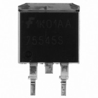
MOSFET N-CH 80V 75A D2PAK

HUF75545S3ST

Manufacturer Part Number
HUF75545S3ST
Description
MOSFET N-CH 80V 75A D2PAK
Manufacturer
Fairchild Semiconductor
Series
UltraFET™r
Datasheet

Specifications of HUF75545S3ST

Fet Type
MOSFET N-Channel, Metal Oxide
Fet Feature
Logic Level Gate
Rds On (max) @ Id, Vgs
10 mOhm @ 75A, 10V
Drain To Source Voltage (vdss)
80V
Current - Continuous Drain (id) @ 25° C
75A
Vgs(th) (max) @ Id
4V @ 250µA
Gate Charge (qg) @ Vgs
235nC @ 20V
Input Capacitance (ciss) @ Vds
3750pF @ 25V
Power - Max
270W
Mounting Type
Surface Mount
Package / Case
D²Pak, TO-263 (2 leads + tab)
Configuration
Single
Transistor Polarity
N-Channel
Resistance Drain-source Rds (on)
0.0082 Ohms
Drain-source Breakdown Voltage
80 V
Gate-source Breakdown Voltage
+/- 20 V
Continuous Drain Current
75 A
Power Dissipation
270 W
Maximum Operating Temperature
+ 175 C
Mounting Style
SMD/SMT
Minimum Operating Temperature
- 55 C
Lead Free Status / RoHS Status
Lead free / RoHS Compliant
Other names
HUF75545S3ST
HUF75545S3STTR
©2002 Fairchild Semiconductor Corporation
75A, 80V, 0.010 Ohm, N-Channel,
UltraFET
Packaging
Symbol
Absolute Maximum Ratings
Drain to Source Voltage (Note 1) . . . . . . . . . . . . . . . . . . . . . . . . . . . . . . . . . . . . . . . . . . . . . V
Drain to Gate Voltage (R
Gate to Source Voltage . . . . . . . . . . . . . . . . . . . . . . . . . . . . . . . . . . . . . . . . . . . . . . . . . . . . . V
Drain Current
Pulsed Avalanche Rating . . . . . . . . . . . . . . . . . . . . . . . . . . . . . . . . . . . . . . . . . . . . . . . . . . . UIS
Power Dissipation . . . . . . . . . . . . . . . . . . . . . . . . . . . . . . . . . . . . . . . . . . . . . . . . . . . . . . . . . . P
Operating and Storage Temperature . . . . . . . . . . . . . . . . . . . . . . . . . . . . . . . . . . . . . . . T
Maximum Temperature for Soldering
NOTES:
CAUTION: Stresses above those listed in “Absolute Maximum Ratings” may cause permanent damage to the device. This is a stress only rating and operation of the
device at these or any other conditions above those indicated in the operational sections of this specification is not implied.
All Fairchild semiconductor products are manufactured, assembled and tested under ISO9000 and QS9000 quality systems certification.
1. T
Pulsed Drain Current . . . . . . . . . . . . . . . . . . . . . . . . . . . . . . . . . . . . . . . . . . . . . . . . . . . . . I
Derate Above 25
Leads at 0.063in (1.6mm) from Case for 10s. . . . . . . . . . . . . . . . . . . . . . . . . . . . . . . . . . . . T
Package Body for 10s, See Techbrief TB334. . . . . . . . . . . . . . . . . . . . . . . . . . . . . . . . . . . T
Continuous (T
Continuous (T
J
= 25
JEDEC TO-220AB
HUF75545P3
Product reliability information can be found at http://www.fairchildsemi.com/products/discrete/reliability/index.html
o
C to 150
(FLANGE)
®
DRAIN
(FLANGE)
DRAIN
Power MOSFET
C
C
o
= 25
= 100
C . . . . . . . . . . . . . . . . . . . . . . . . . . . . . . . . . . . . . . . . . . . . . . . . . . . . . . . . .
SOURCE
o
C.
JEDEC TO-262AA
GS
o
G
C, V
o
DRAIN
C, V
GATE
= 20k ) (Note 1) . . . . . . . . . . . . . . . . . . . . . . . . . . . . . . . . . . .V
GS
GS
= 10V) (Figure 2) . . . . . . . . . . . . . . . . . . . . . . . . . . . . . . . . . I
D
S
= 10V) (Figure 2) . . . . . . . . . . . . . . . . . . . . . . . . . . . . . . . . I
SOURCE
SOURCE
GATE
HUF75545S3
T
Data Sheet
GATE
For severe environments, see our Automotive HUFA series.
C
JEDEC TO-263AB
HUF75545S3S
DRAIN
= 25
o
C, Unless Otherwise Specified
HUF75545P3, HUF75545S3, HUF75545S3S
(FLANGE)
DRAIN
Features
• Ultra Low On-Resistance
• Simulation Models
• Peak Current vs Pulse Width Curve
• UIS Rating Curve
Ordering Information
NOTE: When ordering, use the entire part number. Add the suffix T to
obtain the TO-263AB variant in tape and reel, e.g., HUF75545S3ST.
HUF75545P3
HUF75545S3
HUF75545S3S
- r
- Temperature Compensated PSPICE® and SABER™
- Spice and SABER Thermal Impedance Models
- www.fairchildsemi.com
PART NUMBER
Electrical Models
DS(ON)
J
, T
DGR
DSS
STG
pkg
DM
GS
= 0.010
D
D
D
L
HUF75545P3, HUF75545S3,
TO-220AB
TO-262AA
TO-263AB
V
HUF75545P3 / HUF75545S3 / HUF75545S3S Rev. C
PACKAGE
GS
HUF75545S3S
-55 to 175
Figure 4
Figure 6
10V
270
300
260
September 2002
1.8
80
80
75
73
20
75545P
75545S
75545S
BRAND
UNITS
W/
o
o
o
W
V
V
V
A
A
C
C
C
o
C

Related parts for HUF75545S3ST

HUF75545S3ST Summary of contents

Page 1

... Peak Current vs Pulse Width Curve • UIS Rating Curve Ordering Information PART NUMBER HUF75545P3 HUF75545S3 HUF75545S3S NOTE: When ordering, use the entire part number. Add the suffix T to obtain the TO-263AB variant in tape and reel, e.g., HUF75545S3ST Unless Otherwise Specified September 2002 = 0.010 10V V ...

Page 2

... Gate to Drain “Miller” Charge CAPACITANCE SPECIFICATIONS Input Capacitance Output Capacitance Reverse Transfer Capacitance Source to Drain Diode Specifications PARAMETER Source to Drain Diode Voltage Reverse Recovery Time Reverse Recovered Charge ©2002 Fairchild Semiconductor Corporation Unless Otherwise Specified SYMBOL TEST CONDITIONS 250 (Figure 11) ...

Page 3

... SINGLE PULSE 0. FIGURE 3. NORMALIZED MAXIMUM TRANSIENT THERMAL IMPEDANCE 2000 1000 V = 10V GS 100 TRANSCONDUCTANCE MAY LIMIT CURRENT IN THIS REGION ©2002 Fairchild Semiconductor Corporation 150 175 25 125 o C) FIGURE 2. MAXIMUM CONTINUOUS DRAIN CURRENT RECTANGULAR PULSE DURATION ( PULSE WIDTH (s) FIGURE 4. PEAK CURRENT CAPABILITY ...

Page 4

... PULSE DURATION = DUTY CYCLE = 0.5% MAX 2.0 1.5 1.0 0.5 -80 - JUNCTION TEMPERATURE ( J FIGURE 9. NORMALIZED DRAIN TO SOURCE ON RESISTANCE vs JUNCTION TEMPERATURE ©2002 Fairchild Semiconductor Corporation (Continued) 100 s 1ms 10ms o C 100 200 NOTE: Refer to Fairchild Application Notes AN9321 and AN9322. FIGURE 6. UNCLAMPED INDUCTIVE SWITCHING - ...

Page 5

... I = 250 A D 1.1 1.0 0.9 0.8 -80 - JUNCTION TEMPERATURE ( J FIGURE 11. NORMALIZED DRAIN TO SOURCE BREAKDOWN VOLTAGE vs JUNCTION TEMPERATURE FIGURE 13. GATE CHARGE WAVEFORMS FOR CONSTANT GATE CURRENT ©2002 Fairchild Semiconductor Corporation (Continued) 80 120 160 200 o C) FIGURE 12. CAPACITANCE vs DRAIN TO SOURCE VOLTAGE 40V WAVEFORMS IN 2 DESCENDING ORDER: ...

Page 6

... Test Circuits and Waveforms VARY t TO OBTAIN P R REQUIRED PEAK FIGURE 14. UNCLAMPED ENERGY TEST CIRCUIT g(REF) FIGURE 16. GATE CHARGE TEST CIRCUIT FIGURE 18. SWITCHING TIME TEST CIRCUIT ©2002 Fairchild Semiconductor Corporation DUT 0. DUT g(REF DUT DSS FIGURE 15. UNCLAMPED ENERGY WAVEFORMS Q g(TOT) ...

Page 7

... S2BMOD VSWITCH (RON = 1e-5 ROFF = 0.1 VON = 0.5 VOFF= -1.5) .ENDS NOTE: For further discussion of the PSPICE model, consult A New PSPICE Sub-Circuit for the Power MOSFET Featuring Global Temperature Options; IEEE Power Electronics Specialist Conference Records, 1991, written by William J. Hepp and C. Frank Wheatley. ©2002 Fairchild Semiconductor Corporation DPLCAP 10 RSLC2 ...

Page 8

... Fairchild Semiconductor Corporation DPLCAP 10 RSLC2 - 6 ESG 8 EVTHRES + ...

Page 9

... Fairchild Semiconductor Corporation JUNCTION th RTHERM1 CTHERM1 6 RTHERM2 CTHERM2 5 RTHERM3 CTHERM3 4 RTHERM4 CTHERM4 3 RTHERM5 ...

Page 10

... TRADEMARKS The following are registered and unregistered trademarks Fairchild Semiconductor owns or is authorized to use and is not intended exhaustive list of all such trademarks. ACEx™ FACT™ ActiveArray™ FACT Quiet Series™ ® Bottomless™ FAST CoolFET™ FASTr™ CROSSVOLT™ ...

Related keywords