NTD4863N-35G ON Semiconductor, NTD4863N-35G Datasheet - Page 2
NTD4863N-35G
Manufacturer Part Number
NTD4863N-35G
Description
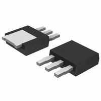
MOSFET N-CH 25V 9.2A IPAK
Manufacturer
ON Semiconductor
Datasheet
1.NTD4863NT4G.pdf
(8 pages)
Specifications of NTD4863N-35G
Fet Type
MOSFET N-Channel, Metal Oxide
Fet Feature
Logic Level Gate
Rds On (max) @ Id, Vgs
9.3 mOhm @ 30A, 10V
Drain To Source Voltage (vdss)
25V
Current - Continuous Drain (id) @ 25° C
9.2A
Vgs(th) (max) @ Id
2.5V @ 250µA
Gate Charge (qg) @ Vgs
13.5nC @ 4.5V
Input Capacitance (ciss) @ Vds
990pF @ 12V
Power - Max
1.27W
Mounting Type
Through Hole
Package / Case
IPak, TO-251, DPak (3 straight short leads + tab)
Lead Free Status / RoHS Status
Lead free / RoHS Compliant
Available stocks
Company
Part Number
Manufacturer
Quantity
Price
Company:

Part Number:
NTD4863N-35G
Manufacturer:
ON Semiconductor
Quantity:
1 858


1. Surface--mounted on FR4 board using 1 sq--in pad, 1 oz Cu.
2. Surface--mounted on FR4 board using the minimum recommended pad size.
THERMAL RESISTANCE MAXIMUM RATINGS
ELECTRICAL CHARACTERISTICS
OFF CHARACTERISTICS
ON CHARACTERISTICS (Note 3)
CHARGES AND CAPACITANCES
SWITCHING CHARACTERISTICS (Note 4)
3. Pulse Test: pulse width ≤ 300 ms, duty cycle ≤ 2%.
4. Switching characteristics are independent of operating junction temperatures.
Junction--to--Case (Drain)
Junction--to--TAB (Drain)
Junction--to--Ambient – Steady State (Note 1)
Junction--to--Ambient – Steady State (Note 2)
Drain--to--Source Breakdown Voltage
Drain--to--Source Breakdown Voltage
Temperature Coefficient
Zero Gate Voltage Drain Current
Gate--to--Source Leakage Current
Gate Threshold Voltage
Negative Threshold Temperature
Coefficient
Drain--to--Source On Resistance
Forward Transconductance
Input Capacitance
Output Capacitance
Reverse Transfer Capacitance
Total Gate Charge
Threshold Gate Charge
Gate--to--Source Charge
Gate--to--Drain Charge
Total Gate Charge
Turn--On Delay Time
Rise Time
Turn--Off Delay Time
Fall Time
Turn--On Delay Time
Rise Time
Turn--Off Delay Time
Fall Time
Parameter
Parameter
(T
J
= 25°C unless otherwise specified)
V
V
V
Symbol
Q
Q
V
GS(TH)
(BR)DSS
R
t
t
(BR)DSS
Q
t
t
d(OFF)
d(OFF)
C
C
I
I
G(TOT)
d(ON)
d(ON)
GS(TH)
C
G(TOT)
Q
Q
GSS
DS(on)
DSS
g
G(TH)
T
OSS
RSS
t
t
t
t
ISS
FS
GS
GD
r
f
r
f
J
/T
/
http://onsemi.com
J
V
V
V
GS
GS
GS
V
V
V
V
V
= 0 V, f = 1.0 MHz, V
V
= 4.5 V, V
= 10 V, V
V
2
DS
GS
V
GS
V
GS
GS
GS
V
I
I
DS
D
D
GS
GS
DS
= 20 V
= 4.5 V
= 15 A, R
= 15 A, R
= 0 V,
= 10 V
= 11.5 V, V
Test Condition
= 4.5 V, V
= 0 V, V
= V
= 0 V, I
= 1.5 V, I
DS
DS
DS
, I
= 15 V, I
D
GS
= 15 V, I
D
G
G
DS
= 250 mA
DS
D
= 250 mA
= 3.0 Ω
= 3.0 Ω
= ±20 V
= 15 A
= 15 V,
= 15 V,
T
T
J
I
I
J
D
D
DS
D
= 125°C
D
= 25°C
= 30 A
= 30 A
= 30 A
= 30 A
= 12 V
R
Symbol
θJC--TAB
R
R
R
θJC
θJA
θJA
Min
1.45
25
17.8
19.7
13.5
16.5
20.2
11.5
Typ
12.8
990
253
144
3.6
7.0
2.0
23
5.0
8.4
9.0
1.0
3.4
4.1
Value
118
4.1
3.5
77
±100
Max
13.5
1.0
10
2.5
9.3
14
mV/°C
mV/°C
°C/W
Unit
Unit
mΩ
mA
nA
nC
ns
ns
nC
pF
V
V
S
Related parts for NTD4863N-35G
Image
Part Number
Description
Manufacturer
Datasheet
Request
R

Part Number:
Description:
MOSFET N-CH 25V 9.2A IPAK
Manufacturer:
ON Semiconductor
Datasheet:

Part Number:
Description:
Power Mosfet 25 V, 49 A, Single N-channel, Dpak/ipak
Manufacturer:
ON Semiconductor
Datasheet:
Part Number:
Description:
ON Semiconductor [VOLTAGE REGULATOR]
Manufacturer:
ON Semiconductor
Datasheet:
Part Number:
Description:
357-036-542-201 CARDEDGE 36POS DL .156 BLK LOPRO
Manufacturer:
ON Semiconductor
Datasheet:
Part Number:
Description:
357-036-542-201 CARDEDGE 36POS DL .156 BLK LOPRO
Manufacturer:
ON Semiconductor
Datasheet:
Part Number:
Description:
357-036-542-201 CARDEDGE 36POS DL .156 BLK LOPRO
Manufacturer:
ON Semiconductor
Datasheet:
Part Number:
Description:
357-036-542-201 CARDEDGE 36POS DL .156 BLK LOPRO
Manufacturer:
ON Semiconductor
Datasheet:
Part Number:
Description:
357-036-542-201 CARDEDGE 36POS DL .156 BLK LOPRO
Manufacturer:
ON Semiconductor
Datasheet:
Part Number:
Description:
357-036-542-201 CARDEDGE 36POS DL .156 BLK LOPRO
Manufacturer:
ON Semiconductor
Datasheet:
Part Number:
Description:
357-036-542-201 CARDEDGE 36POS DL .156 BLK LOPRO
Manufacturer:
ON Semiconductor
Datasheet:
Part Number:
Description:
357-036-542-201 CARDEDGE 36POS DL .156 BLK LOPRO
Manufacturer:
ON Semiconductor
Datasheet:
Part Number:
Description:
357-036-542-201 CARDEDGE 36POS DL .156 BLK LOPRO
Manufacturer:
ON Semiconductor
Datasheet:
Part Number:
Description:
357-036-542-201 CARDEDGE 36POS DL .156 BLK LOPRO
Manufacturer:
ON Semiconductor
Datasheet:
Part Number:
Description:
Manufacturer:
ON Semiconductor
Datasheet: