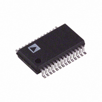
AD977ABRS Analog Devices Inc, AD977ABRS Datasheet - Page 8

AD977ABRS
Manufacturer Part Number
AD977ABRS
Description
ADC Single SAR 200KSPS 16-Bit Serial 28-Pin SSOP
Manufacturer
Analog Devices Inc
Datasheet
1.AD977ARZ.pdf
(24 pages)
Specifications of AD977ABRS
Package
28SSOP
Resolution
16 Bit
Sampling Rate
200 KSPS
Architecture
SAR
Number Of Analog Inputs
1
Digital Interface Type
Serial
Input Type
Voltage
Signal To Noise Ratio
85(Min) dB
Polarity Of Input Voltage
Unipolar|Bipolar
Rohs Status
RoHS non-compliant
Number Of Bits
16
Sampling Rate (per Second)
200k
Data Interface
Serial, SPI™
Number Of Converters
1
Power Dissipation (max)
100mW
Voltage Supply Source
Analog and Digital
Operating Temperature
-40°C ~ 85°C
Mounting Type
Surface Mount
Package / Case
28-SSOP (0.200", 5.30mm Width)
For Use With
EVAL-AD977CB - BOARD EVAL FOR AD977EVAL-AD977ACB - BOARD EVAL FOR AD977A
Lead Free Status / RoHS Status
Available stocks
Company
Part Number
Manufacturer
Quantity
Price
Part Number:
AD977ABRS
Manufacturer:
ADI/亚德诺
Quantity:
20 000
Company:
Part Number:
AD977ABRSZ
Manufacturer:
CRYSTEK
Quantity:
30 000
Part Number:
AD977ABRSZ
Manufacturer:
ADI/亚德诺
Quantity:
20 000
AD977/AD977A
CONVERSION CONTROL
The AD977/AD977A is controlled by two signals: R/C and CS.
When R/C is brought low, with CS low, for a minimum of 50 ns,
the input signal will be held on the internal capacitor array and
a conversion “n” will begin. Once the conversion process does
begin, the BUSY signal will go low until the conversion is com-
plete. Internally, the signals R/C and CS are OR’d together and
there is no requirement on which signal is taken low first when
initiating a conversion. The only requirement is that there be at
least 10 ns of delay between the two signals being taken low.
After the conversion is complete the BUSY signal will return
high and the AD977/AD977A will again resume tracking the
input signal. Under certain conditions the CS pin can be tied
Low and R/C will be used to determine whether you are initiat-
ing a conversion or reading data. On the first conversion, after
the AD977/AD977A is powered up, the DATA output will be
indeterminate.
Conversion results can be clocked serially out of the AD977/
AD977A using either an internal clock, generated by the
AD977/AD977A, or by using an external clock. The AD977/
AD977A is configured for the internal data clock mode by pull-
ing the EXT/INT pin low. It is configured for the external clock
mode by pulling the EXT/INT pin high.
DATACLK
CS, R/C
MODE
BUSY
DATA
BUSY
R/C
ACQUIRE
t
2
t
1
t
8
t
2
t
10
t
5
t
1
MSB VALID
1
t
9
CONVERT
t
BIT 14
VALID
11
2
t
6
t
INTERNAL DATA CLOCK MODE
The AD977/AD977A is configured to generate and provide the
data clock when the EXT/INT pin is held low. Typically CS will
be tied low and R/C will be used to initiate a conversion “n.”
During the conversion the AD977/AD977A will output 16 bits of
data, MSB first, from conversion “n-1” on the DATA pin. This
data will be synchronized with 16 clock pulses provided on the
DATACLK pin. The output data will be valid on both the
rising and falling edge of the data clock as shown in Figure 3.
After the LSB has been presented, the DATA pin will assume
whatever state the TAG input was at during the start of con-
version, and the DATACLK pin will stay low until another
conversion is initiated.
EXTERNAL DATA CLOCK MODE
The AD977/AD977A is configured to accept an externally sup-
plied data clock when the EXT/INT pin is held high. This mode
of operation provides several methods by which conversion
results can be read from the AD977/AD977A. The output data
from conversion “n-1” can be read during conversion “n,” or the
output data from conversion “n” can be read after the conver-
sion is complete. The external clock can be either a continuous
or discontinuous clock. A discontinuous clock can be either
3
t
6
BIT 13
VALID
3
t
4
ACQUIRE
t
7
VALID
BIT 1
15
CS
LSB VALID
16
CONVERT
INT


