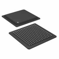
ADSP-21061LKBZ-160 Analog Devices Inc, ADSP-21061LKBZ-160 Datasheet - Page 4

ADSP-21061LKBZ-160
Manufacturer Part Number
ADSP-21061LKBZ-160
Description
DSP Floating-Point 32-Bit 40MHz 40MIPS 225-Pin BGA
Manufacturer
Analog Devices Inc
Series
SHARC®r
Type
Floating Pointr
Datasheet
1.ADSP-21061LKSZ-160.pdf
(56 pages)
Specifications of ADSP-21061LKBZ-160
Package
225BGA
Numeric And Arithmetic Format
Floating-Point
Maximum Speed
40 MHz
Ram Size
128 KB
Device Million Instructions Per Second
40 MIPS
Interface
Synchronous Serial Port (SSP)
Clock Rate
40MHz
Non-volatile Memory
External
On-chip Ram
128kB
Voltage - I/o
3.30V
Voltage - Core
3.30V
Operating Temperature
0°C ~ 85°C
Mounting Type
Surface Mount
Package / Case
225-BGA
Lead Free Status / RoHS Status
Lead free / RoHS Compliant
Available stocks
Company
Part Number
Manufacturer
Quantity
Price
Company:
Part Number:
ADSP-21061LKBZ-160
Manufacturer:
Analog Devices Inc
Quantity:
10 000
ADSP-21061/ADSP-21061L
GENERAL DESCRIPTION
The ADSP-21061 SHARC—Super Harvard Architecture Com-
puter—is a signal processing microcomputer that offers new
capabilities and levels of performance. The ADSP-21061
SHARC is a 32-bit processor optimized for high performance
DSP applications. The ADSP-21061 builds on the ADSP-21000
DSP core to form a complete system-on-a-chip, adding a dual-
ported on-chip SRAM and integrated I/O peripherals supported
by a dedicated I/O bus.
Fabricated in a high speed, low power CMOS process, the
ADSP-21061 has a 20 ns instruction cycle time and operates at
40 MIPS. With its on-chip instruction cache, the processor can
execute every instruction in a single cycle.
mance benchmarks for the ADSP-21061/ADSP-21061L.
The ADSP-21061 SHARC represents a new standard of integra-
tion for signal computers, combining a high performance
floating-point DSP core with integrated, on-chip system fea-
tures including 1M bit SRAM memory, a host processor
interface, a DMA controller, serial ports, and parallel bus con-
nectivity for glueless DSP multiprocessing.
Table 1. Benchmarks (at 50 MHz)
The ADSP-21061 continues SHARC’s industry-leading stan-
dards of integration for DSPs, combining a high performance
32-bit DSP core with integrated, on-chip system features.
The block diagram
tural features:
Benchmark Algorithm
1024 Point Complex FFT (Radix 4,
with reversal)
FIR Filter (per tap)
IIR Filter (per biquad)
Divide (y/x)
Inverse Square Root
DMA Transfer Rate
• Computation units (ALU, multiplier, and shifter) with a
• Data address generators (DAG1, DAG2)
• Program sequencer with instruction cache
• PM and DM buses capable of supporting four 32-bit data
• Interval timer
• On-chip SRAM
• External port for interfacing to off-chip memory and
• Host port and multiprocessor interface
• DMA controller
shared data register file
transfers between memory and the core at every core pro-
cessor cycle
peripherals
on Page
1, illustrates the following architec-
Speed
.37 ms
20 ns
80 ns
120 ns
180 ns
300M Bps
Table 1
shows perfor-
Cycles
18,221
1
4
6
9
Rev. C | Page 4 of 56 | July 2007
SHARC FAMILY CORE ARCHITECTURE
The ADSP-21061 includes the following architectural features
of the ADSP-21000 family core. The ADSP-21061 processors
are code- and function-compatible with the ADSP-21020,
ADSP-21060, and ADSP-21062 SHARC processors.
Independent, Parallel Computation Units
The arithmetic/logic unit (ALU), multiplier, and shifter all per-
form single-cycle instructions. The three units are arranged in
parallel, maximizing computational throughput. Single multi-
function instructions execute parallel ALU and multiplier oper-
ations. These computation units support IEEE 32-bit single-
precision floating-point, extended-precision 40-bit floating-
point, and 32-bit fixed-point data formats.
Data Register File
A general-purpose data register file is used for transferring data
between the computation units and the data buses, and for stor-
ing intermediate results. This 10-port, 32-register (16 primary,
16 secondary) register file, combined with the ADSP-21000
Harvard architecture, allows unconstrained data flow between
computation units and internal memory.
• Serial ports
• JTAG test access port
(OPTIONAL)
1
(OPTIONAL)
DEVICE
SERIAL
TO GND
SERIAL
DEVICE
CLOCK
Figure 2. ADSP-21061/ADSP-21061L System Sample Configuration
3
4
CLKIN
EBOOT
LBOOT
FLAG
TIMEXP
TCLK0
RCLK0
TFS0
RSF0
DT0
DR0
TCLK1
RCLK1
TFS1
RSF1
DT1
DR1
RPBA
ID
IRQ
2–0
RESET
2–0
ADSP-21061
3–0
ADDR
DATA
DMAR
DMAG
ADRCLK
JTAG
MS
PAGE
REDY
BR
SBTS
BMS
HBG
ACK
HBR
CPA
31–0
47–0
7
WR
SW
3–0
RD
1–2
1–2
CS
1–6
DATA
CS
ADDR
DATA
ADDR
DATA
OE
WE
ACK
CS
ADDR
DATA
PROCESSOR
(OPTIONAL)
INTERFACE
DMA DEVICE
(OPTIONAL)
(OPTIONAL)
(OPTIONAL)
MEMORY-
HOST
DEVICES
MAPPED
EPROM
BOOT


