MW6S010NR1 Freescale Semiconductor, MW6S010NR1 Datasheet - Page 6
MW6S010NR1
Manufacturer Part Number
MW6S010NR1
Description
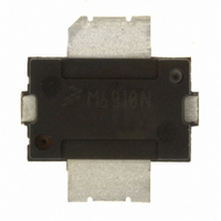
MOSFET RF N-CH 28V 10W TO-270-2
Manufacturer
Freescale Semiconductor
Datasheet
1.MW6S010NR1.pdf
(20 pages)
Specifications of MW6S010NR1
Transistor Type
N-Channel
Frequency
960MHz
Gain
18dB
Voltage - Rated
68V
Current Rating
10µA
Current - Test
125mA
Voltage - Test
28V
Power - Output
10W
Package / Case
TO-270-2
Configuration
Dual
Transistor Polarity
N-Channel
Drain-source Breakdown Voltage
68 V
Gate-source Breakdown Voltage
12 V
Continuous Drain Current
125 mA
Power Dissipation
10 W
Maximum Operating Temperature
+ 150 C
Mounting Style
SMD/SMT
Minimum Operating Temperature
- 65 C
Channel Type
N
Channel Mode
Enhancement
Drain Source Voltage (max)
68V
Power Gain (typ)@vds
20dB
Frequency (max)
1.5GHz
Package Type
TO-270
Pin Count
3
Output Capacitance (typ)@vds
10@28VpF
Reverse Capacitance (typ)
0.32@28VpF
Operating Temp Range
-65C to 225C
Drain Efficiency (typ)
33%
Mounting
Surface Mount
Mode Of Operation
2-Tone
Number Of Elements
1
Power Dissipation (max)
61400mW
Vswr (max)
10
Screening Level
Military
Drain Source Voltage Vds
68V
Rf Transistor Case
TO-270
Msl
MSL 3 - 168 Hours
Filter Terminals
SMD
Peak Reflow Compatible (260 C)
Yes
Rohs Compliant
Yes
Operating Frequency Max
900MHz
Gate-source Voltage
12V
Leaded Process Compatible
Yes
Lead Free Status / RoHS Status
Lead free / RoHS Compliant
Noise Figure
-
Lead Free Status / Rohs Status
Lead free / RoHS Compliant
Other names
MW6S010NR1
MW6S010NR1TR
MW6S010NR1TR
Available stocks
Company
Part Number
Manufacturer
Quantity
Price
Company:

Part Number:
MW6S010NR1
Manufacturer:
OMRON
Quantity:
2 300
Part Number:
MW6S010NR1
Manufacturer:
FREESCALE
Quantity:
20 000


MW6S010NR1 MW6S010GNR1
6
19
18
17
16
15
0
Figure 10. Power Gain versus Output Power
2
P
out
4
, OUTPUT POWER (WATTS) CW
6
8
50
40
30
20
10
20
19
18
17
16
15
0
V
0.1
0.1
DD
10
T
= 24 V
25_C
Figure 8. Single - Carrier CDMA ACPR, Power
85_C
TYPICAL CHARACTERISTICS
C
G
V
I
f = 945 MHz
= −30_C
DQ
ps
DD
Figure 9. Power Gain and Power Added
= 125 mA
= 28 Vdc
Gain and Power Added Efficiency
12
Efficiency versus Output Power
28 V
I
f = 945 MHz
DQ
P
P
out
= 125 mA
out
14
, OUTPUT POWER (WATTS) AVG.
versus Output Power
, OUTPUT POWER (WATTS) CW
1
32 V
G
η
ps
D
16
1
−30_C
24
20
16
12
8
4
0
500
ACPR
Figure 11. Broadband Frequency Response
10
V
P
I
DQ
DD
out
600
η
— 900 MHz
D
= 125 mA
= 28 Vdc
= 10 W CW
V
I
f = 945 MHz
DQ
DD
25_C
700
= 125 mA
= 28 Vdc
85_C
f, FREQUENCY (MHz)
100
800
10
−10
−20
−30
−40
−50
−60
50
40
30
20
10
0
900
S11
S21
1000
Freescale Semiconductor
1100
RF Device Data
1200
5
0
−5
−10
−15
−20
−25
Related parts for MW6S010NR1
Image
Part Number
Description
Manufacturer
Datasheet
Request
R

Part Number:
Description:
RF Power Field Effect Transistor
Manufacturer:
Freescale Semiconductor
Datasheet:


Part Number:
Description:
RELAY HI FREQ 6GHZ DPDT
Manufacturer:
TE Connectivity
Datasheet:

Part Number:
Description:
Manufacturer:
Freescale Semiconductor, Inc
Datasheet:
Part Number:
Description:
Manufacturer:
Freescale Semiconductor, Inc
Datasheet:
Part Number:
Description:
Manufacturer:
Freescale Semiconductor, Inc
Datasheet:
Part Number:
Description:
Manufacturer:
Freescale Semiconductor, Inc
Datasheet:
Part Number:
Description:
Manufacturer:
Freescale Semiconductor, Inc
Datasheet:
Part Number:
Description:
Manufacturer:
Freescale Semiconductor, Inc
Datasheet:
Part Number:
Description:
Manufacturer:
Freescale Semiconductor, Inc
Datasheet:
Part Number:
Description:
Manufacturer:
Freescale Semiconductor, Inc
Datasheet:
Part Number:
Description:
Manufacturer:
Freescale Semiconductor, Inc
Datasheet:
Part Number:
Description:
Manufacturer:
Freescale Semiconductor, Inc
Datasheet:
Part Number:
Description:
Manufacturer:
Freescale Semiconductor, Inc
Datasheet:
Part Number:
Description:
Manufacturer:
Freescale Semiconductor, Inc
Datasheet: