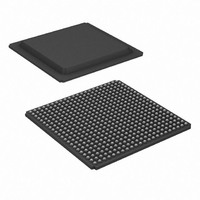
XC3S1600E-4FGG484I Xilinx Inc, XC3S1600E-4FGG484I Datasheet - Page 213

XC3S1600E-4FGG484I
Manufacturer Part Number
XC3S1600E-4FGG484I
Description
FPGA Spartan®-3E Family 1.6M Gates 33192 Cells 572MHz 90nm (CMOS) Technology 1.2V 484-Pin FBGA
Manufacturer
Xilinx Inc
Series
Spartan™-3Er
Datasheet
1.XC3S100E-4VQG100C.pdf
(233 pages)
Specifications of XC3S1600E-4FGG484I
Package
484FBGA
Family Name
Spartan®-3E
Device Logic Cells
33192
Device Logic Units
3688
Device System Gates
1600000
Number Of Registers
29504
Maximum Internal Frequency
572 MHz
Typical Operating Supply Voltage
1.2 V
Maximum Number Of User I/os
376
Ram Bits
663552
Number Of Logic Elements/cells
33192
Number Of Labs/clbs
3688
Total Ram Bits
663552
Number Of I /o
376
Number Of Gates
1600000
Voltage - Supply
1.14 V ~ 1.26 V
Mounting Type
Surface Mount
Operating Temperature
-40°C ~ 100°C
Package / Case
484-BBGA
Lead Free Status / RoHS Status
Lead free / RoHS Compliant
For Use With
HW-XA3S1600E-UNI-G - KIT DEVELOPMENT AUTOMOTIVE ECU
Lead Free Status / RoHS Status
Lead free / RoHS Compliant
Available stocks
Company
Part Number
Manufacturer
Quantity
Price
Company:
Part Number:
XC3S1600E-4FGG484I
Manufacturer:
XILINX
Quantity:
140
Company:
Part Number:
XC3S1600E-4FGG484I
Manufacturer:
XILINX
Quantity:
250
Company:
Part Number:
XC3S1600E-4FGG484I
Manufacturer:
Xilinx Inc
Quantity:
10 000
Part Number:
XC3S1600E-4FGG484I
Manufacturer:
XILINX/赛灵思
Quantity:
20 000
User I/Os by Bank
Table 149
pins are distributed between the four I/O banks on the
FG320 package.
Table 149: User I/Os Per Bank for XC3S500E in the FG320 Package
Table 150: User I/Os Per Bank for XC3S1200E and XC3S1600E in the FG320 Package
DS312-4 (v3.8) August 26, 2009
Product Specification
Notes:
1.
2.
Notes:
1.
2.
Top
Right
Bottom
Left
TOTAL
Top
Right
Bottom
Left
TOTAL
Package
Package
Some VREF and CLK pins are on INPUT pins.
The eight global clock pins in this bank have optional functionality during configuration and are counted in the DUAL column.
Some VREF and CLK pins are on INPUT pins.
The eight global clock pins in this bank have optional functionality during configuration and are counted in the DUAL column.
Edge
Edge
and
R
Table 150
I/O Bank
I/O Bank
0
1
2
3
0
1
2
3
indicate how the available user-I/O
Maximum
Maximum
232
250
I/O
I/O
58
58
58
58
61
63
63
63
102
120
I/O
I/O
29
22
17
34
34
25
23
38
www.xilinx.com
INPUT
INPUT
14
10
13
11
48
12
12
11
12
47
All Possible I/O Pins by Type
All Possible I/O Pins by Type
DUAL
DUAL
21
24
46
21
24
46
1
0
1
0
VREF
VREF
20
21
6
5
4
5
6
5
5
5
Pinout Descriptions
(1)
(1)
CLK
CLK
0
0
0
0
16
16
8
8
(2)
(2)
8
8
(2)
(2)
(1)
(1)
213


