CV210-3AF TriQuint, CV210-3AF Datasheet

Up-Down Converters CNVRTR DUAL BRNCH HI-SDE LO 800-960MHZ

CV210-3AF

Manufacturer Part Number
CV210-3AF
Description
Up-Down Converters CNVRTR DUAL BRNCH HI-SDE LO 800-960MHZ
Manufacturer
TriQuint
Type
Down Converterr
Datasheet

Specifications of CV210-3AF

If Frequency
200 MHz to 350 MHz
Noise Figure
10.3 dB
P1db
10 dBm
Rf Frequency
800 MHz to 960 MHz
Lead Free Status / RoHS Status
Lead free / RoHS Compliant
Other names
1066943

Available stocks

Company
Part Number
Manufacturer
Quantity
Price
Part Number:
CV210-3AF
Manufacturer:
TriQuint
Quantity:
1 122
Part Number:
CV210-3AF
Manufacturer:
WJ
Quantity:
20 000
CV210-3A
Cellular-band Dual-Branch Downconverter
Product Features
Specifications
1. Specifications when using the application specific circuit (shown on page 3) with a low side LO = 0 dBm and IF = 240 MHz in a downconverting application at 25° C.
2. IF matching components affect the center IF frequency. Proper component values for other IF center frequencies than shown can be provided by emailing to applications.engineering@wj.com.
3. The IF bandwidth of the converter is defined as 15% around any center frequency in its operating IF frequency range. The bandwidth is determined with external components. Specifications are valid around
4. Assumes the supply voltage = +5 V. IIP3 is measured with Δf = 1 MHz with RF
5. Assumes LO injection noise is filtered at the thermal noise floor, -174 dBm/Hz, at the RF, IF, and Image frequencies.
6. The maximum junction temperature ensures a minimum MTTF rating of 1 million hours of usage.
Absolute Maximum Rating
Operation of this device above any of these parameters may cause permanent damage.
TriQuint Semiconductor, Inc • Phone +1-503-615-9000 • FAX: +1-503-615-8900 • e-mail: info-sales@tqs.com • Web site: www.TriQuint.com
Parameters
RF Frequency Range
LO Frequency Range
IF Center Frequency Range
% Bandwidth around IF center frequency
IF Test Frequency
SSB Conversion Gain
Gain Drift over Temp (-40° C to 85° C)
Input IP3
Input IP2
Input 1 dB Compression Point
Noise Figure
LO Input Drive Level
LO-RF Isolation
LO-IF Isolation
Branch-Branch Isolation
Return Loss: RF Port
Return Loss: LO Port
Return Loss: IF Port
Operating Supply Voltage
Supply Current
Thermal Resistance
Junction Temperature
Parameter
Operating Case Temperature
Storage Temperature
DC Voltage
Junction Temperature
High dynamic range downconverter
with integrated LO and IF amplifiers
Dual channels for diversity
+29 dBm Input IP3
+10 dBm Input P1dB
RF: 800 – 960 MHz
IF: 200 – 350 MHz
+5V Single supply operation
Pb-free 6mm 28-pin QFN package
High-side LO configuration
Common footprint with other
PCS/UMTS/cellular versions
the total ±7.5% bandwidth. ie. with a center frequency of 240 MHz, the specifications are valid from 240 ± 18 MHz.
(1)
Rating
-40° to +85° C
-55° to +150° C
+5.5 V
+220 °C
The CV210-3A is a dual-channel high-linearity down-
converter designed to meet the demanding performance,
functionality, and cost goals of current and next generation
mobile infrastructure basestations. It provides high
dynamic range performance in a low profile lead-
free/RoHS-compliant surface-mount leadless package that
measures 6x6 mm square.
It is ideally suited for high dynamic range receiver front
ends using diversity receive channels. Functionality
includes frequency conversion and IF amplification, while
an integrated LO driver amplifier powers the passive
mixer.
mature GaAs MESFET and InGaP HBT technology.
Typical applications include frequency downconversion
used in CDMA/GSM/TDMA, CDMA2000, W-CDMA,
and EDGE 2.5G and 3G mobile base transceiver stations.
Units
°C / W
MHz
MHz
MHz
MHz
dBm
dBm
dBm
dBm
mA
dB
dB
dB
dB
dB
dB
dB
dB
dB
°C
%
V
The MCM is implemented with reliable and
Product Description
in
= -5 dBm / tone.
Min
-1.5
+25
+33
-2.5
320
8
Ordering Information
1000 – 1310
Part No.
CV210-3AF
CV210-3APCB240 Fully-Assembled Application Board, IF = 240MHz
800 – 960
200 – 350
Typ
±7.5
10.3
±0.3
10.3
+29
+40
240
+10
390
+5
14
34
60
17
14
12
0
Specifications and information are subject to change without notice
Description
Cellular-band Dual-Branch Downconverter
(lead-free/RoHS-compliant 6x6mm QFN package)
Max
+2.5
475
160
1.5
12
27
GND
BIAS
GND
GND
Functional Diagram
N/C
N/C
N/C
1
2
3
4
5
6
7
Comments
See note 2
See note 3
Temp = 25° C
Referenced to +25° C
See note 4
See note 4
See note 4
See note 5
P
P
See note 6
LO
LO
28
8
= 0 dBm
= 0 dBm
27
9
RF/IF
RF/IF
Top View
26
10
25
11
IF Amp 1
IF Amp 2
LO Driver Amp
24
12
Page 1 of 6 April 2010
23
13
22
14
21
20
19
18
17
16
15
BIAS
GND
N/C
GND
LO
GND
N/C

Related parts for CV210-3AF

CV210-3AF Summary of contents

Page 1

... 320 390 ° ° dBm / tone. in Ordering Information Part No. CV210-3AF CV210-3APCB240 Fully-Assembled Application Board 240MHz Functional Diagram RF/IF N/C 1 GND 2 IF Amp 1 BIAS 3 GND 4 N Driver Amp GND 6 IF Amp 2 N/C 7 RF/ Top View ...

Page 2

... CV210-3A: The application circuit can be broken up into three main functions as denoted in the colored dotted areas above: RF/IF diplexing (blue), IF amplifier matching (green), and dc biasing (purple). placeholders for chip components in the circuit schematic so that a common PCB can be used for all WJ dual-branch converters. Further details are given in the Application Note located on the website titled “ ...

Page 3

... CV210-3A Cellular-band Dual-Branch Downconverter Application Circuit 240 MHz (CV210-3APCB240) PCB Layout Circuit Board Material: .014” FR-4, 4 layers, .062” total thickness TriQuint Semiconductor, Inc • Phone +1-503-615-9000 • FAX: +1-503-615-8900 • e-mail: info-sales@tqs.com • Web site: www.TriQuint.com Ref. Desig. R1 R2, R3, R4, C16 ...

Page 4

... CV210-3A Cellular-band Dual-Branch Downconverter CV210-3APCB240 Application Circuit Performance Plots Conversion Gain vs IF Frequency dBm, 1090 MHz -40° C +25° C +85° 215 225 235 245 255 IF Frequency (MHz) Conversion Gain vs RF Frequency 25° 240 MHz, high-side -2.5 dBm dBm LO = 2.5 dBm ...

Page 5

... CV210-3A Cellular-band Dual-Branch Downconverter CV210-3APCB240 Application Circuit Performance Plots L-R Isolation vs LO Frequency Referenced with dBm -40° C +25° C +85° 900 1000 1100 1200 1300 LO Frequency (MHz) IF Return Loss vs IF Frequency 25° 215 225 235 245 255 IF Frequency (MHz) TriQuint Semiconductor, Inc • Phone +1-503-615-9000 • FAX: +1-503-615-8900 • e-mail: info-sales@tqs.com • Web site: www.TriQuint.com ...

Page 6

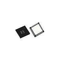
... CV210-3A Cellular-band Dual-Branch Downconverter CV210-3AF Mechanical Information This package is lead-free/RoHS-compliant compatible with both lead-free (maximum 260°C reflow temperature) and leaded (maximum 245°C reflow temperature) soldering processes. The plating material on the pins is annealed matte tin over copper. Outline Drawing Mounting Configuration / Land Pattern TriQuint Semiconductor, Inc • ...

Related keywords