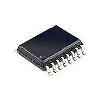
CY2309SC-1T Cypress Semiconductor Corp, CY2309SC-1T Datasheet

CY2309SC-1T
Specifications of CY2309SC-1T
Available stocks
Related parts for CY2309SC-1T
CY2309SC-1T Summary of contents
Page 1
... PLL REF S2 Select Input Decoding S1 Cypress Semiconductor Corporation Document #: 38-07140 Rev. *G Low-Cost 3.3V Zero Delay Buffer CY2309. It accepts one reference input, and drives out five low-skew clocks. The -1H versions of each device operate 100-/133-MHz frequencies, and have higher drive than the -1 devices. All parts have on-chip PLLs which lock to an input clock on the REF pin ...
Page 2
Pin Description for CY2309 Pin Signal [1] 1 REF [2] 2 CLKA1 [2] 3 CLKA2 GND [2] 6 CLKB1 [2] 7 CLKB2 [ [ [2] 10 CLKB3 [2] 11 CLKB4 12 GND ...
Page 3
REF. Input to CLKA/CLKB Delay vs. Loading Difference between CLKOUT and CLKA/CLKB Pins Zero Delay and Skew Control All outputs should be uniformly loaded to achieve Zero Delay between the input and output. Since the CLKOUT pin is the internal ...
Page 4
... Absolute Maximum Conditions Supply Voltage to Ground Potential ............... –0.5V to +7.0V DC Input Voltage (Except REF) ............–0. Input Voltage REF......................................... –0. Operating Conditions for CY2305SC-XX and CY2309SC-XX Commercial Temperature Devices Parameter V Supply Voltage DD T Operating Temperature (Ambient Temperature Load Capacitance, below 100 MHz L C Load Capacitance, from 100 MHz to 133 MHz ...
Page 5
... Switching Characteristics for CY2305SC-1H and CY2309SC-1H Commercial Temperature Devices Parameter Name t1 Output Frequency [6] ÷ t Duty Cycle = [6] ÷ t Duty Cycle = [6] t3 Rise Time [6] t Fall Time 4 [6] t Output to Output Skew 5 t Delay, REF Rising Edge to 6A [6] CLKOUT Rising Edge t Delay, REF Rising Edge to ...
Page 6
Switching Characteristics for CY2305SI-1and CY2309SI-1 Industrial Temperature Devices Parameter Name t1 Output Frequency [6] ÷ t Duty Cycle = [6] t3 Rise Time [6] t Fall Time 4 [6] t Output to Output Skew 5 t Delay, ...
Page 7
Switching Waveforms Duty Cycle Timing 1.4V 1.4V All Outputs Rise/Fall Time 2.0V 2.0V OUTPUT 0. Output-Output Skew 1.4V OUTPUT 1.4V OUTPUT t 5 Input-Output Propagation Delay INPUT OUTPUT ...
Page 8
Typical Duty Cycle and I Trends DD Duty Cycle Vs VDD (for 30 pF Loads over Frequency - 3.3V, 25C 3.1 3.2 3.3 3.4 3.5 VDD (V) ...
Page 9
Typical Duty Cycle and IDD Trends Duty Cycle Vs VDD (for 30 pF Loads over Frequency - 3.3V, 25C 3.1 3.2 3.3 3.4 VDD (V) Duty Cycle ...
Page 10
... SOIC – (Lead-free) CY2305SXI-1HT 8-pin 150-mil SOIC – Tape and Reel – (Lead-free) CY2309SC-1 16-pin 150-mil SOIC CY2309SC-1T 16-pin 150-mil SOIC – Tape and Reel CY2309SZC-1 16-pin 150-mil SOIC – (Lead-free) CY2309SZC-1T 16-pin 150-mil SOIC – Tape and Reel – (Lead-free) CY2309SXC-1 16-pin 150-mil SOIC – ...
Page 11
... SOIC – (Lead-free) CY2309SXI-1T 16-pin 150-mil SOIC – Tape and Reel – (Lead-free) CY2309SC-1H 16-pin 150-mil SOIC CY2309SC-1HT 16-pin 150-mil SOIC – Tape and Reel CY2309SZC-1H 16-pin 150-mil SOIC – (Lead-free) CY2309SZC-1HT 16-pin 150-mil SOIC – Tape and Reel – (Lead-free) CY2309SXC-1H 16-pin 150-mil SOIC – ...
Page 12
Package Drawing and Dimensions 8 Lead (150 Mil) SOIC - S08 0.189[4.800] 0.196[4.978] 0.050[1.270] BSC 0.0138[0.350] 0.0192[0.487] 16 Lead (150 Mil) SOIC 8 9 0.386[9.804] 0.393[9.982] 0.050[1.270] BSC 0.0138[0.350] 0.0192[0.487] Document #: 38-07140 Rev. *G 8-lead ...
Page 13
... Document #: 38-07140 Rev. *G © Cypress Semiconductor Corporation, 2005. The information contained herein is subject to change without notice. Cypress Semiconductor Corporation assumes no responsibility for the use of any circuitry other than circuitry embodied in a Cypress product. Nor does it convey or imply any license under patent or other rights. Cypress products are not warranted nor intended to be used for medical, life support, life saving, critical control or safety applications, unless pursuant to an express written agreement with Cypress ...
Page 14
... HWT Added eight-pin TSSOP packages (CY2305ZC-1 and CY2305ZC-1T) to the ordering information table. Added the Tape and Reel option to all the existing packages: CY2305SC-1T, CY2305SI-1T, CY2305SC-1HT, CY2305SI-1HT, CY2305ZC-1T, CY2309SC-1T, CY2309SI-1T, CY2309SC-1HT, CY2309SI-1HT, CY2309ZC-1HT, CY2309ZI-1HT RBI Power-up requirements added to Operating Conditions information RGL ...


