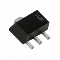
PBSS4540X,135 NXP Semiconductors, PBSS4540X,135 Datasheet - Page 5

PBSS4540X,135
Manufacturer Part Number
PBSS4540X,135
Description
TRANS PNP 40V 4A SOT89
Manufacturer
NXP Semiconductors
Series
-r
Specifications of PBSS4540X,135
Package / Case
SC-62, SOT-89, TO-243 (3 Leads + Tab)
Transistor Type
NPN
Current - Collector (ic) (max)
4A
Voltage - Collector Emitter Breakdown (max)
40V
Vce Saturation (max) @ Ib, Ic
355mV @ 500mA, 5A
Current - Collector Cutoff (max)
100nA
Dc Current Gain (hfe) (min) @ Ic, Vce
250 @ 2A, 2V
Power - Max
1.6W
Frequency - Transition
70MHz
Mounting Type
Surface Mount
Dc Collector/base Gain Hfe Min
300
Minimum Operating Temperature
- 65 C
Configuration
Single
Transistor Polarity
NPN
Mounting Style
SMD/SMT
Collector- Emitter Voltage Vceo Max
40 V
Emitter- Base Voltage Vebo
6 V
Continuous Collector Current
4 A
Maximum Dc Collector Current
10 A
Power Dissipation
550 mW
Maximum Operating Frequency
70 MHz
Maximum Operating Temperature
+ 150 C
Lead Free Status / RoHS Status
Lead free / RoHS Compliant
Lead Free Status / RoHS Status
Lead free / RoHS Compliant, Lead free / RoHS Compliant
Other names
934057105135
PBSS4540X /T3
PBSS4540X /T3
PBSS4540X /T3
PBSS4540X /T3
NXP Semiconductors
THERMAL CHARACTERISTICS
Notes
1. Pulse test: t
2. Device mounted on a printed-circuit board, single-sided copper, tin-plated and standard footprint.
3. Device mounted on a printed-circuit board, single-sided copper, tin-plated and mounting pad for collector 1 cm
4. Device mounted on a printed-circuit board, single-sided copper, tin-plated and mounting pad for collector 6 cm
5. Device mounted on a 7 cm
2004 Nov 04
R
R
40 V, 5 A
PNP low V
th(j-a)
th(j-s)
Mounted on FR4 printed-circuit board; standard footprint.
(1) δ = 1.
(2) δ = 0.75.
SYMBOL
(K/W)
Z
10
th
10
10
10
−1
1
3
2
10
−5
p
≤ 10 ms; δ ≤ 0.2.
thermal resistance from junction to
ambient
thermal resistance from junction to
soldering point
CEsat
(3) δ = 0.5.
(4) δ = 0.33.
Fig.3 Transient thermal impedance as a function of pulse time; typical values.
10
−4
(10)
(1)
(2)
(3)
(4)
(5)
(6)
(7)
(8)
(9)
(BISS) transistor
2
PARAMETER
ceramic printed-circuit board, 1 cm
10
−3
(5) δ = 0.2.
(6) δ = 0.1.
10
−2
(7) δ = 0.05.
(8) δ = 0.02.
10
5
−1
in free air
notes 1 and 2
note 2
note 3
note 4
note 5
CONDITIONS
2
(9) δ = 0.01.
(10) δ = 0.
single-sided copper and tin-plated.
1
10
VALUE
225
125
10
50
90
80
16
2
PBSS5540X
Product data sheet
t
p
006aaa232
(s)
10
UNIT
3
K/W
K/W
K/W
K/W
K/W
K/W
2
2
.
.


