DDTA143ZE-7-F Diodes Inc, DDTA143ZE-7-F Datasheet

TRANS PREBIASED PNP 150MW SOT523

DDTA143ZE-7-F

Manufacturer Part Number
DDTA143ZE-7-F
Description
TRANS PREBIASED PNP 150MW SOT523
Manufacturer
Diodes Inc
Datasheet

Specifications of DDTA143ZE-7-F

Transistor Type
PNP - Pre-Biased
Current - Collector (ic) (max)
100mA
Voltage - Collector Emitter Breakdown (max)
50V
Resistor - Base (r1) (ohms)
4.7K
Resistor - Emitter Base (r2) (ohms)
47K
Dc Current Gain (hfe) (min) @ Ic, Vce
80 @ 10mA, 5V
Vce Saturation (max) @ Ib, Ic
300mV @ 250µA, 5mA
Frequency - Transition
250MHz
Power - Max
150mW
Mounting Type
Surface Mount
Package / Case
SOT-523
Lead Free Status / RoHS Status
Lead free / RoHS Compliant
Other names
DDTA143ZE-FDITR
Mechanical Data
Features
Maximum Ratings
Supply Voltage, (2) to (3)
Input Voltage, (1) to (2)
Output Current
Output Current
Notes:
DS30318 Rev. 7 – 2
Epitaxial Planar Die Construction
Complementary NPN Types Available (DDTC)
Built-In Biasing Resistors, R1≠R2
Lead Free Finish/RoHS Compliant (Note 1)
"Green" Device (Note 2 and 3)
Case: SOT-523
Case Material: Molded Plastic. UL Flammability
Classification Rating 94V-0
Moisture Sensitivity: Level 1 per J-STD-020C
Terminals: Solderable per MIL-STD-202, Method 208
Lead Free Plating (Matte Tin Finish annealed over Alloy 42
leadframe).
Terminal Connections: See Diagram
Marking & Date Code Information: See Diagrams & Page 4
Ordering Information: See Page 4
Weight: 0.002 grams (approximate)
DDTA113ZE
DDTA123YE
DDTA123JE
DDTA143XE
DDTA143FE
DDTA143ZE
DDTA114YE
DDTA114WE
DDTA124XE
DDTA144VE
DDTA144WE
1. No purposefully added lead.
2. Diodes Inc.'s "Green" policy can be found on our website at http://www.diodes.com/products/lead_free/index.php.
3. Product manufactured with Date Code UO (week 40, 2007) and newer are built with Green Molding Compound. Product manufactured prior to Date
P/N
Code UO are built with Non-Green Molding Compound and may contain Halogens or Sb2O3 Fire Retardants.
R1 (NOM)
2.2KΩ
2.2KΩ
4.7KΩ
4.7KΩ
4.7KΩ
10KΩ
10KΩ
22KΩ
47KΩ
47KΩ
1KΩ
Characteristic
@T
A
= 25°C unless otherwise specified
R2 (NOM)
4.7KΩ
10KΩ
10KΩ
47KΩ
10KΩ
22KΩ
47KΩ
47KΩ
47KΩ
10KΩ
22KΩ
DDTA113ZE
DDTA113ZE
DDTA123YE
DDTA123JE
DDTA143ZE
DDTA114WE
DDTA144VE
DDTA144WE
DDTA123YE
DDTA123JE
DDTA114YE
DDTA114WE
DDTA144VE
DDTA144WE
DDTA143XE
DDTA143FE
DDTA114YE
DDTA124XE
DDTA143XE
DDTA143FE
DDTA143ZE
DDTA124XE
Marking
P02
P05
P06
P09
P10
P11
P14
P15
P18
P21
P22
All
PNP PRE-BIASED SMALL SIGNAL SURFACE MOUNT TRANSISTOR
www.diodes.com
K
J
1 of 4
DDTA (R1≠R2 SERIES) E
Schematic and Pin Configuration
TOP VIEW
G
H
A
Symbol
I
C
D
IN
1
V
B
V
(Max)
I
CC
O
IN
R1
OUT
3
B
C
N
R2
C
L
GND(+)
2
E
+10 to -30
+10 to -40
+15 to -40
+10 to -40
+5 to -10
+5 to -12
+5 to -12
+7 to -20
+6 to -30
+5 to -30
+6 to -40
Value
M
-100
-100
-100
-100
-100
-100
-100
-100
-50
-70
-50
-30
-30
IN
Dim
Equivalent Inverter Circuit
B
A
B
C
D
G
H
K
M
N
J
L
α
All Dimensions in mm
DDTA (R1≠R2 SERIES) E
1
0.15
0.75
1.45
0.90
1.50
0.00
0.60
0.10
0.10
0.45
Min
GND (+)
SOT-523
E
© Diodes Incorporated
Max
0.30
0.85
1.75
1.10
1.70
0.10
0.80
0.30
0.20
0.65
3
Unit
mA
mA
V
V
C
0.22
0.80
1.60
0.50
1.00
1.60
0.05
0.75
0.22
0.12
0.50
Typ
OUT

Related parts for DDTA143ZE-7-F

DDTA143ZE-7-F Summary of contents

Page 1

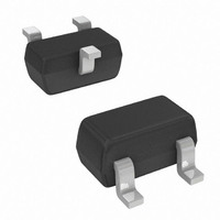
... Schematic and Pin Configuration P21 P22 Symbol V CC DDTA113ZE DDTA123YE DDTA123JE DDTA143XE DDTA143FE DDTA143ZE V IN DDTA114YE DDTA114WE DDTA124XE DDTA144VE DDTA144WE DDTA113ZE DDTA123YE DDTA123JE DDTA143XE DDTA143FE DDTA143ZE I O DDTA114YE DDTA114WE DDTA124XE DDTA144VE DDTA144WE All I (Max www.diodes.com SOT-523 Dim Min A 0. 0.75 C 1.45 D — ...

Page 2

... DDTA143ZE DDTA114YE DDTA114WE DDTA124XE DDTA144VE DDTA144WE Output Current DDTA113ZE DDTA123YE DDTA123JE DDTA143XE DDTA143FE DC Current Gain DDTA143ZE DDTA114YE DDTA114WE DDTA124XE DDTA144VE DDTA144WE Input Resistor Tolerance Resistance Ratio Tolerance Gain-Bandwidth Product* * Transistor – For Reference Only DS30318 Rev. 7 – 25°C unless otherwise specified A ...

Page 3

... DS30318 Rev. 7 – 2 TYPICAL CURVES - DDTA123JE 1 0.1 0.01 0.001 100 150 ° 100 www.diodes.com COLLECTOR CURRENT (mA) C Fig vs. I CE(SAT 1MHz REVERSE BIAS VOLTAGE (V) R Fig. 4 Output Capacitance COLLECTOR CURRENT (mA) C Fig. 6 Input Voltage vs. Collector Current DDTA (R1≠R2 SERIES) E © Diodes Incorporated ...

Page 4

... Ordering Information (Note 5) Device DDTA113ZE-7-F DDTA123YE-7-F DDTA123JE-7-F DDTA143XE-7-F DDTA143FE-7-F DDTA143ZE-7-F DDTA114YE-7-F DDTA114WE-7-F DDTA124XE-7-F DDTA144VE-7-F DDTA144WE-7-F Notes: 5. For packaging details our website at http://www.diodes.com/datasheets/ap02007.pdf. Marking Information Date Code Key Year 2005 2006 Code S Month Jan Feb Code 1 2 Diodes Incorporated and its subsidiaries reserve the right to make modifications, enhancements, improvements, corrections or other changes without further notice to any product herein. Diodes Incorporated does not assume any liability arising out of the application or use of any product described herein ...

Related keywords