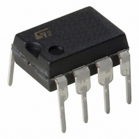
ACS110-7SB2 STMicroelectronics, ACS110-7SB2 Datasheet

ACS110-7SB2
Specifications of ACS110-7SB2
Available stocks
Related parts for ACS110-7SB2
ACS110-7SB2 Summary of contents
Page 1
... It is triggered with a negative gate current flowing out of the gate pin. April 2003 - Ed +/-700V RRM = 1A T(RMS) < back on the FUNCTIONAL DIAGRAM ACS110-7SN/SB2 AC LINE SWITCH COM OUT COM G SOT-223 ACS110-7SN G OUT COM COM COM COM DIL-8 ACS110-7SB2 OUT COM G 1/10 ...
Page 2
... ACS110-7SN/SB2 ABSOLUTE RATINGS (limiting values) For either positive or negative polarity of pin OUT voltage in respect to pin COM voltage Symbol Repetitive peak off-state voltage DRM RRM I RMS on-state current full cycle sine wave T(RMS Non repetitive surge peak on-state current TSM Tj initial = 25°C, full cycle sine wave ...
Page 3
... L R =140 QII - QIII Tj=25°C L Tj=125°C Tj=25°C Tj=25°C Tj=25°C Tj=125°C Tj=125°C Tj=25°C Tj=125°C Tj=110°C Tj=125°C Tj=25°C ACS110-7SN/SB2 Values Unit MAX 10 mA MAX 1 V MIN 0.15 V MAX 45 mA MAX 65 mA MAX 1 ...
Page 4
... Several ACS110 devices can be connected on the same cooling PCB pad, which is the COM pin. Thanks to its thermal and turn off commutation performances, the ACS110 switch is able to drive with no turn off additional snubber an inductive load ...
Page 5
... OUT AC LINE TRANSIENT VOLTAGE RUGGEDNESS The ACS110 switch is able to sustain safely the AC line transient voltages either by clamping the low en- ergy spikes or by breaking over under high energy shocks, even with high turn-on current rises. The test circuit of the figure C is representative of the final ACS application and is also used to stress the ACS switch according to the IEC 61000-4-5 standard conditions ...
Page 6
... ACS110-7SN/SB2 OTHER FIGURES Maximum power dissipation vs RMS on state current. RMS on-state current vs ambient temperature, case temperature and package Relative variation of thermal impedance junction to ambient vs pulse duration and package Relative variation of gate trigger current vs junction temperature Relative variation of holding and latching current vs junction ...
Page 7
... Fig. 9: Non repetitive surge peak on-state current for a sinusoidal pulse with width tp < 10ms, and corresponding value of I²t. I TSM 100.0 t=20ms 10.0 1.0 0.1 100 1000 0.01 ACS110-7SN/SB2 (° 100 (° 100 (A), I²t (A²s) t (ms) p 0.10 1.00 V =460V OUT ...
Page 8
... ACS110-7SN/SB2 Fig. 10: On-state characteristics (maximum values). I (A) TM 10.00 T max =0. =300m d 1.00 T =125° =25°C j 0.10 V (V) TM 0.01 0.0 0.5 1.0 1.5 2.0 ORDERING INFORMATION AC Switch Number of switches 8/10 Fig. 11: Thermal resistance junction to ambient versus copper surface under tab (printed circuit board FR4, copper thickness: 35µm) ...
Page 9
... GATE BASE c 0.24 2 DRAIN COLLECTOR D 6.30 SOURCE EMITTER 3 4 DRAIN COLLECTOR 3.30 H 6.70 V ACS110-7SN/SB2 DIMENSIONS Millimeters Inches Typ. Max. Min. Typ. 1.80 0.10 0.001 0.70 0.85 0.024 0.027 0.033 3.00 3.15 0.114 0.118 0.124 0.26 0.35 0.009 0.010 0.014 6.50 6.70 ...
Page 10
... Ordering type Marking ACS110-7SN ACS1107S ACS110-7SB2 ACS1107S Epoxy meets UL94,V0 Information furnished is believed to be accurate and reliable. However, STMicroelectronics assumes no responsibility for the consequences of use of such information nor for any infringement of patents or other rights of third parties which may result from its use. No license is granted by implication or otherwise under any patent or patent rights of STMicroelectronics ...


