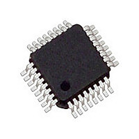
CY29942AC Cypress Semiconductor Corp, CY29942AC Datasheet

CY29942AC
Specifications of CY29942AC
Available stocks
Related parts for CY29942AC
CY29942AC Summary of contents
Page 1
... Available in Industrial and Commercial ■ 32-pin LQFP package Logic Block Diagram Cypress Semiconductor Corporation Document #: 38-07284 Rev. *D 2.5V or 3.3V, 200 MHz, 1:18 Clock Description The CY29942 is a low voltage 200 MHz clock distribution buffer with an LVCMOS or LVTTL compatible input clock. All other control inputs are LVCMOS/LVTTL compatible ...
Page 2
Pinouts [1] Table 1. Pin Description Pin Name 3 TCLK 10, 11, 13, 14, 15, 18, 19, 20, Q(17:0) 22, 23, 24, 26, 27, 28, 30, 31 16, 21, 29 VDD 1, 2, 12, ...
Page 3
Maximum Ratings [2] Maximum Input Voltage Relative to V :............. V SS Maximum Input Voltage Relative to V :............. V DD Storage Temperature: ...................................... –65° to 150°C Operating Temperature:..................................... –40° to 85°C Maximum ESD protection............................................... 2 kV Maximum Power Supply:................................................ ...
Page 4
AC Parameters V = 3.3V ±5% or 2.5V ±5 3.3V ±5% or 2.5V ±5%, Over the specified temperature range DD DDC Parameter Description Fmax Input Frequency Tpd TTL_CLK to Q Delay [ FoutDC Output Duty Cycle ...
Page 5
... Figure 5. Ordering Information Part Number CY29942AI 32-Pin LQFP CY29942AIT 32-Pin LQFP – Tape and Reel CY29942AC 32-Pin LQFP Pb-free CY29942AXI 32-Pin LQFP CY29942AXIT 32-Pin LQFP – Tape and Reel CY29942AXC 32-Pin LQFP CY29942AXCT 32-Pin LQFP – Tape and Reel Document #: 38-07284 Rev. *D Figure 4 ...
Page 6
Package Drawing and Dimensions 32-Pin Thin Plastic Quad Flatpack 1.4 mm A32.14 Document #: 38-07284 Rev. *D CY29942 51-85088-*B Page [+] Feedback ...
Page 7
... New datasheet Added a Commercial Temp. Range in the Ordering Information Add power up requirements to maximum rating information. Added Lead-free devices Added typical value for output-output skew Ordering Information table: fixed typo and removed obsolete CY29942ACT. Changed Lead-free to Pb-free. psoc.cypress.com clocks.cypress.com image.cypress.com Revised September 10, 2009 ...


