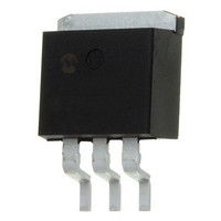
MCP1825S-5002E/EB Microchip Technology, MCP1825S-5002E/EB Datasheet - Page 17

MCP1825S-5002E/EB
Manufacturer Part Number
MCP1825S-5002E/EB
Description
500 MA CMOS LDO, Vout=5.0V, Extended Temp Range 3 DDPAK TUBE
Manufacturer
Microchip Technology
Datasheet
1.MCP1825T-ADJEDC.pdf
(38 pages)
Specifications of MCP1825S-5002E/EB
Regulator Topology
Positive Fixed
Voltage - Output
5V
Voltage - Input
Up to 6V
Voltage - Dropout (typical)
0.21V @ 500mA
Number Of Regulators
1
Current - Output
500mA (Min)
Operating Temperature
-40°C ~ 125°C
Mounting Type
Surface Mount
Package / Case
TO-263-3, D²Pak (3 leads + Tab), TO-263AA
Number Of Outputs
1
Polarity
Positive
Input Voltage Max
6 V
Output Voltage
5 V
Output Type
Fixed
Dropout Voltage (max)
0.35 V at 500 mA
Output Current
500 mA
Line Regulation
0.05 % / V
Load Regulation
0.5 %
Voltage Regulation Accuracy
0.5 %
Maximum Operating Temperature
+ 125 C
Mounting Style
SMD/SMT
Minimum Operating Temperature
- 40 C
Lead Free Status / RoHS Status
Lead free / RoHS Compliant
Current - Limit (min)
-
Lead Free Status / Rohs Status
Lead free / RoHS Compliant
4.0
The MCP1825/MCP1825S is a high output current,
Low Dropout (LDO) voltage regulator. The low dropout
voltage of 210 mV typical at 500 mA of current makes
it ideal for battery-powered applications. Unlike other
high output current LDOs, the MCP1825/MCP1825S
only draws a maximum of 220 µA of quiescent current.
The MCP1825 has a shutdown control input and a
power good output.
4.1
The 5-pin MCP1825 LDO is available with either a fixed
output voltage or an adjustable output voltage. The
output voltage range is 0.8V to 5.0V for both versions.
The 3-pin MCP1825S LDO is available as a fixed
voltage device.
4.1.1
The adjustable version of the MCP1825 uses the ADJ
pin (pin 5) to get the output voltage feedback for output
voltage regulation. This allows the user to set the
output voltage of the device with two external resistors.
The nominal voltage for ADJ is 0.41V.
Figure 4-1
MCP1825. Resistors R
divider network necessary to set the output voltage.
With this configuration, the equation for setting V
EQUATION 4-1:
FIGURE 4-1:
voltage application circuit.
The allowable resistance value range for resistor R
from 10 kΩ to 200 kΩ. Solving the equation for R
yields the following equation:
© 2008 Microchip Technology Inc.
Off
Where:
On
V
V
OUT
ADJ
DEVICE OVERVIEW
LDO Output Voltage
SHDN
V
IN
ADJUST INPUT
shows the adjustable version of the
4.7 µF
C
1
=
=
V
OUT
MCP1825-ADJ
1
LDO Output Voltage
ADJ Pin Voltage
(typically 0.41V)
2
=
Typical adjustable output
3 4 5
GND
V
1
ADJ
and R
⎛
⎝
ADJ
R
------------------
1
R
+
2
2
R
form the resistor
2
⎞
⎠
R
R
V
1
2
OUT
OUT
1 µF
C2
2
is:
is
1
MCP1825/MCP1825S
EQUATION 4-2:
4.2
The MCP1825/MCP1825S LDO is tested and ensured
to supply a minimum of 500 mA of output current. The
MCP1825/MCP1825S has no minimum output load, so
the output load current can go to 0 mA and the LDO will
continue to regulate the output voltage to within
tolerance.
The MCP1825/MCP1825S also incorporates an output
current limit. If the output voltage falls below 0.7V due
to an overload condition (usually represents a shorted
load condition), the output current is limited to 1.2A
(typical). If the overload condition is a soft overload, the
MCP1825/MCP1825S will supply higher load currents
of up to 1.5A. The MCP1825/MCP1825S should not be
operated in this condition continuously as it may result
in failure of the device. However, this does allow for
device usage in applications that have higher pulsed
load currents having an average output current value of
500 mA or less.
Output overload conditions may also result in an over-
temperature shutdown of the device. If the junction
temperature rises above 150°C, the LDO will shut
down the output voltage. See Section 4.8 “Overtem-
perature Protection” for more information on
overtemperature shutdown.
4.3
The MCP1825/MCP1825S requires a minimum output
capacitance of 1 µF for output voltage stability.
Ceramic capacitors are recommended because of their
size, cost and environmental robustness qualities.
Aluminum-electrolytic and tantalum capacitors can be
used on the LDO output as well. The Equivalent Series
Resistance (ESR) of the electrolytic output capacitor
must be no greater than 1 ohm. The output capacitor
should be located as close to the LDO output as is
practical. Ceramic materials X7R and X5R have low
temperature coefficients and are well within the
acceptable ESR range required. A typical 1 µF X7R
0805 capacitor has an ESR of 50 milli-ohms.
Larger LDO output capacitors can be used with the
MCP1825/MCP1825S
performance and power supply ripple rejection
performance. A maximum of 22 µF is recommended.
Aluminum-electrolytic capacitors are not recom-
mended for low temperature applications of < -25°C.
Where:
V
V
OUT
ADJ
Output Current and Current
Limiting
Output Capacitor
=
=
R
1
LDO Output Voltage
ADJ Pin Voltage
(typically 0.41V)
=
R
2
⎛
⎝
V
--------------------------------
OUT
to
V
ADJ
–
V
improve
ADJ
DS22056B-page 17
⎞
⎠
dynamic


