PI6C182HEX Pericom Semiconductor, PI6C182HEX Datasheet
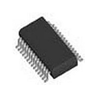
Clock Buffer Precision 1 12 Clock Buffer

PI6C182HEX

Manufacturer Part Number
PI6C182HEX
Description
Clock Buffer Precision 1 12 Clock Buffer
Manufacturer
Pericom Semiconductor
Datasheet

Specifications of PI6C182HEX

Number Of Outputs
10
Max Input Freq
110 MHz
Propagation Delay (max)
5.5 ns
Supply Voltage (max)
3.465 V
Supply Voltage (min)
3.135 V
Maximum Operating Temperature
+ 70 C
Minimum Operating Temperature
0 C
Mounting Style
SMD/SMT
Package / Case
SSOP-28
Operating Supply Voltage (max)
3.465V
Operating Temp Range
0C to 70C
Propagation Delay Time
8ns
Operating Supply Voltage (min)
3.135V
Mounting
Surface Mount
Pin Count
28
Operating Supply Voltage (typ)
3.3V
Package Type
SSOP
Input Frequency
110MHz
Duty Cycle
55%
Operating Temperature Classification
Commercial
Lead Free Status / RoHS Status
Compliant
Lead Free Status / RoHS Status
Lead free / RoHS Compliant, Compliant
Features
• Low noise non-inverting 1-to-10 buffer
• Supports frequency up to 125 MHz (PI6C182A)
• Supports up to four SDRAM DIMMs
• Low skew (<200ps) between any two output clocks
• I
• Multiple V
• 3.3V power supply voltage
• Separate Hi-Z state pin for testing
• Packaging (Pb-free & Green available):
Diagram
— 28-pin SSOP (H)
2
C Serial Confi guration interface
BUF_IN
08-0298
DD
SCLOCK
and V
SDATA
OE
SS
pins for noise reduction
I 2 C
I/O
SDRAM0
SDRAM1
SDRAM2
SDRAM3
SDRAM9
1
Description
The PI6C182 is a high-speed low-noise 1-to-10 noninverting buf-
fer designed for SDRAM clock buffer applications, supporting
frequencies up to 110 MHz.
At power up all SDRAM output are enabled and active. The I
serial control may be used to individually activate/de ac ti vate any
driver.
The output enable pin (OE) may be pulled LOW to tri-state all
outputs.
Note:
Purchases of I
use in I
Pin Con fi g u ra tion
2
C system defi ned by Philips Semiconductor.
SDRAM1
SDRAM2
SDRAM3
SDRAM8
SDRAM0
BUF_IN
V DDIIC
SDATA
V DD2
V DD0
V DD1
V SS1
V SS2
V SS0
2
C components from Pericom conveys a license of
Precision 1-to-10 Clock Buffer
1
2
3
4
5
6
7
8
9
10
11
12
13
14
28
27
26
25
24
23
22
21
20
19
18
17
16
15
V DD5
SDRAM7
SDRAM6
V SS5
V DD4
SDRAM5
SDRAM4
V SS4
OE
V DD3
SDRAM9
V SS3
V SSIIC
SCLOCK
PI6C182A
PS8165G
PI6C182
11/13/08
2
C

Related parts for PI6C182HEX

PI6C182HEX Summary of contents

Page 1

Features • Low noise non-inverting 1-to-10 buffer • Supports frequency up to 125 MHz (PI6C182A) • Supports up to four SDRAM DIMMs • Low skew (<200ps) between any two output clocks 2 • Serial Confi guration interface • ...

Page 2

Pin Description Pin Symbol SDRAM[0-3] 22, 23, 26, 27 SDRAM[4-7] 11, 18 SDRAM[8-9] 9 BUF_IN SDATA 15 SCLOCK 1, 5, 10, 19, 24, VDD[0- 12, 17, 21, VSS[0- ...

Page 3

I C Control 2 The I C interface permits individual enable/disable of each clock output and test mode enable. The PI6C182 is a slave receiver device. It can not be read back. Sub-addressing is not supported. All preceding ...

Page 4

DC Operating Specifi cations Symbol Parameter V Input High voltage IH V Input Low voltage IL I Input leakage current IL V Output High voltage OH V Output Low voltage OL C Output pin capacitance OUT C Input pin ...

Page 5

Clocking Interface (TTL) Input Waveform Output Waveform Minimum and Maximum Expected Capacitive Loads Clock Min. Max. Units SDRAM Notes: 1. Maximum rise/fall times are guaranteed at maximum specifi ed load. 2. Minimum rise/fall times are guaranteed ...

Page 6

PCB Layout Suggestion C1 VDD VSS 4 C2 VDD VSS VDD 10 11 VSS 12 C4 VDD 13 14 Notes: 1. This is only a suggested layout. 2. C1-C7 should ...

Page 7

... Packaging Mechanical: 28-Pin SSOP (H) 08-0143 (1,2,3) Ordering Information Ordering Code PI6C182AHE PI6C182AHEX Notes: 1. Thermal characteristics can be found on the company web site at www.pericom.com/packaging Pb-free and Green 3. X Suffi Tape/Reel Pericom Semiconductor Corporation • 1-800-435-2336 • www.pericom.com 08-0298 28-Pin, 209-Mil Wide, SSOP ...

Related keywords