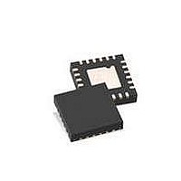
ISP1506ABS,518 NXP Semiconductors, ISP1506ABS,518 Datasheet - Page 18

ISP1506ABS,518
Manufacturer Part Number
ISP1506ABS,518
Description
RF Transceiver USB ULPI TRNSCVR
Manufacturer
NXP Semiconductors
Datasheet
1.ISP1506BBS557.pdf
(80 pages)
Specifications of ISP1506ABS,518
Number Of Transceivers
1
Esd Protection
YeskV
Operating Supply Voltage (typ)
Not RequiredV
Operating Temperature Classification
Industrial
Operating Supply Voltage (max)
Not RequiredV
Operating Supply Voltage (min)
Not RequiredV
Mounting
Surface Mount
Operating Temperature (max)
85C
Operating Temperature (min)
-40C
Operating Supply Voltage
1.65 V to 3.6 V
Mounting Style
SMD/SMT
Package / Case
HVQFN-24
Lead Free Status / RoHS Status
Compliant
Other names
935278332518 ISP1506ABS-T
NXP Semiconductors
Table 6.
ISP1506A_ISP1506B_2
Product data sheet
Signal
TX_ENABLE
DAT
SE0
INT
Signal mapping for 3-pin serial mode
8.1.3 3-pin full-speed or low-speed serial mode
8.2 USB and OTG state transitions
Maps to
DATA0
DATA1
DATA2
DATA3
If the link requires a 3-pin serial interface to transmit and receive full-speed or low-speed
USB data, it can set the ISP1506 to 3-pin serial mode. In 3-pin serial mode, the data bus
definition changes to that shown in
3PIN_FSLS_SERIAL bit in the Interface Control register to logic 1. To exit 3-pin serial
mode, the link asserts STP. This is primarily provided for links that contain legacy
full-speed or low-speed functionality, providing a more cost-effective upgrade path to
high-speed. An interrupt pin is also provided to inform the link of USB events. If the link
requires CLOCK to be running during 3-pin serial mode, the CLOCK_SUSPENDM
register bit must be set to logic 1.
For more information on 3-pin serial mode enter and exit protocols, refer to
Low Pin Interface (ULPI) Specification Rev.
A Hi-Speed USB peripheral, host or OTG device handles more than one electrical state as
defined in
Supplement to the USB 2.0 Specification Rev.
states through register bit settings of XCVRSELECT[1:0], TERMSELECT, OPMODE[1:0],
DP_PULLDOWN and DM_PULLDOWN.
Table 7
resistor settings as also given in
The link is responsible for setting the desired USB and OTG states.
•
•
•
•
RPU_DP_EN enables the 1.5 k pull-up resistor on DP
RPD_DP_EN enables the 15 k pull-down resistor on DP
RPD_DM_EN enables the 15 k pull-down resistor on DM
HSTERM_EN enables the 45
summarizes operating states. The values of register settings in
Ref. 1 “Universal Serial Bus Specification Rev. 2.0”
Direction
I
I/O
I/O
O
Rev. 02 — 28 August 2008
Description
active HIGH transmit enable
transmit differential data on DP and DM when TX_ENABLE is HIGH
receive differential data from DP and DM when TX_ENABLE is LOW
transmit single-ended zero on DP and DM when TX_ENABLE is HIGH
receive single-ended zero from DP and DM when TX_ENABLE is LOW
active HIGH interrupt indication; will be asserted whenever any
unmasked interrupt occurs
Table
Table
termination resistors on DP and DM
7. Resistor setting signals are defined as follows:
6. To enter 3-pin serial mode, the link sets the
1.1”.
ISP1506A; ISP1506B
1.3”. The ISP1506 accommodates various
ULPI HS USB OTG transceiver
and
Ref. 2 “On-The-Go
© NXP B.V. 2008. All rights reserved.
Table 7
Ref. 3 “UTMI+
will force
17 of 79


