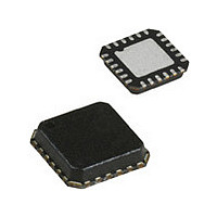
USB3311-CP-TR Standard Microsystems (SMSC), USB3311-CP-TR Datasheet - Page 7

USB3311-CP-TR
Manufacturer Part Number
USB3311-CP-TR
Description
Manufacturer
Standard Microsystems (SMSC)
Datasheet
1.USB3311-CP-TR.pdf
(12 pages)
Specifications of USB3311-CP-TR
Number Of Transceivers
1
Esd Protection
YeskV
Power Supply Requirement
Single
Operating Supply Voltage (typ)
Not RequiredV
Package Type
QFN
Operating Temperature Classification
Industrial
Operating Supply Voltage (max)
Not RequiredV
Operating Supply Voltage (min)
Not RequiredV
Mounting
Surface Mount
Operating Temperature (max)
85C
Operating Temperature (min)
-40C
Lead Free Status / RoHS Status
Compliant
Available stocks
Company
Part Number
Manufacturer
Quantity
Price
Hi-Speed USB Transceiver with 1.8V ULPI Interface - 26MHz Reference Clock
SMSC USB3311
BALL
PIN/
D2
D1
E1
E2
E3
D3
E4
D4
E5
D5
C4
C5
B4
B5
A5
A4
10
11
12
13
14
15
16
17
18
19
4
5
6
7
8
9
SPKR_R/M
CLKOUT
DATA[7]
DATA[6]
DATA[5]
DATA[4]
DATA[3]
DATA[2]
DATA[1]
DATA[0]
SPKR_L
VDD3.3
NAME
NXT
DIR
DM
DP
Table 1 USB3311 Pin Description (continued)
PRODUCT PREVIEW
DIRECTION/
Output,
Output,
Output,
Analog
Analog
Analog
Analog
CMOS
CMOS
CMOS
CMOS
CMOS
CMOS
CMOS
CMOS
CMOS
CMOS
CMOS
Power
TYPE
I/O,
I/O,
I/O,
I/O,
I/O,
I/O,
I/O,
I/O,
I/O,
I/O,
I/O,
I/O,
7
ACTIVE
LEVEL
High
N/A
N/A
N/A
N/A
N/A
N/A
N/A
N/A
N/A
N/A
N/A
N/A
N/A
N/A
N/A
3.3V Regulator Output. A 2.2uF (<1 ohm
ESR) bypass capacitor to ground is
required for regulator stability. The
bypass capacitor should be placed as
close as possible to the USB3311.
D- pin of the USB cable.
D+ pin of the USB cable.
USB switch in/out for DP signals
USB switch in/out for DM signals
ULPI bi-directional data bus. DATA[7] is
the MSB.
ULPI bi-directional data bus.
ULPI bi-directional data bus.
ULPI bi-directional data bus.
60MHz reference clock output. All ULPI
signals are driven synchronous to the
rising edge of this clock.
ULPI bi-directional data bus.
ULPI bi-directional data bus.
ULPI bi-directional data bus.
ULPI bi-directional data bus. DATA[0] is
the LSB.
The PHY asserts NXT to throttle the data.
When the Link is sending data to the
PHY, NXT indicates when the current
byte has been accepted by the PHY. The
Link places the next byte on the data bus
in the following clock cycle.
Controls the direction of the data bus.
When the PHY has data to transfer to the
Link, it drives DIR high to take ownership
of the bus. When the PHY has no data to
transfer it drives DIR low and monitors
the bus for commands from the Link.
DESCRIPTION
Revision 1.3 (11-02-07)


