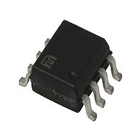
MIC2025-2FBN Micrel Inc, MIC2025-2FBN Datasheet - Page 9

MIC2025-2FBN
Manufacturer Part Number
MIC2025-2FBN
Description
Manufacturer
Micrel Inc
Datasheet
1.MIC2025-2FBN.pdf
(14 pages)
Specifications of MIC2025-2FBN
Short Circuit Current Limit
700mA
Input Voltage Range
2.7 to 5.5V
Number Of Switches
Single
Operating Temp Range
-40C to 85C
Operating Temperature Classification
Industrial
Mounting
Surface Mount
Pin Count
8
Package Type
SOIC
Lead Free Status / RoHS Status
Not Compliant
Block Diagram
Functional Description
Input and Output
IN is the power supply connection to the logic circuitry and
the drain of the output MOSFET. OUT is the source of the
output MOSFET. In a typical circuit, current flows from IN to
OUT toward the load. If V
flow from OUT to IN since the switch is bidirectional when
enabled. The output MOSFET and driver circuitry are also
designed to allow the MOSFET source to be externally forced
to a higher voltage than the drain (V
switch is disabled. In this situation, the MIC2025/75 avoids
undesirable current flow from OUT to IN.
Thermal Shutdown
Thermal shutdown is employed to protect the device from
damage should the die temperature exceed safe margins
due mainly to short circuit faults. Each channel employs its
own thermal sensor. Thermal shutdown shuts off the output
MOSFET and asserts the FLG output if the die temperature
reaches 140°C. The MIC2025 will automatically reset its output
should the die temperature cool down to 120°C. The MIC2025
output and FLG signal will continue to cycle on and off until
the device is disabled or the fault is removed. Figure 2 depicts
typical timing. If the MIC2075 goes into thermal shutdown, its
output will latch off and a pull-up current source is activated.
This allows the output latch to automatically reset when the
load (such as a USB device) is removed. The output can also
be reset by toggling EN. Refer to Figure 1 for details.
Depending on PCB layout, package, ambient temperature,
etc., it may take several hundred milliseconds from the in-
cidence of the fault to the output MOSFET being shut off.
The worst-case scenario of thermal shutdown is that of a
short-circuit fault and is shown in the in the “Function Char-
acteristics: Thermal Shutdown Response” graph.
June 2010
EN
OUT
is greater than V
CHARGE
PUMP
OSC.
OUT
> V
SHUTDOWN
THERMAL
IN
IN
, current will
) when the
GND
UVLO
9
Power Dissipation
The device’s junction temperature depends on several fac-
tors such as the load, PCB layout, ambient temperature
and package type. Equations that can be used to calculate
power dissipation of each channel and junction temperature
are found below.
Total power dissipation of the device will be the summation of
P
the following equation can be used:
where:
Current Sensing and Limiting
The current-limit threshold is preset internally. The preset
level prevents damage to the device and external load but
still allows a minimum current of 500mA to be delivered to
the load.
The current-limit circuit senses a portion of the output MOSFET
switch current. The current-sense resistor shown in the block
diagram is virtual and has no voltage drop. The reaction to
an overcurrent condition varies with three scenarios:
Switch Enabled into Short-Circuit
If a switch is enabled into a heavy load or short-circuit, the
switch immediately enters into a constant-current mode,
reducing the output voltage. The FLG signal is asserted
indicating an overcurrent condition. See the Short-Circuit
Response graph under Functional Characteristics.
D
for both channels. To relate this to junction temperature,
CONTROL
GATE
P
T
T
T
θ
A
JA
J
J
D
= P
= junction temperature
= ambient temperature
= R
REFERENCE
= is the thermal resistance of the package
D
1.2V
DS(on)
× θ
RESPONSE
DELAY
FLAG
JA
CURRENT
× I
LIMIT
+ T
OUT
A
2
IN
OUT
FLG
MIC2025/2075


