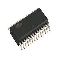
STK11C48-N35 Cypress Semiconductor Corp, STK11C48-N35 Datasheet - Page 2

STK11C48-N35
Manufacturer Part Number
STK11C48-N35
Description
Manufacturer
Cypress Semiconductor Corp
Type
NVSRAMr
Datasheet
1.STK11C48-N35.pdf
(3 pages)
Specifications of STK11C48-N35
Word Size
8b
Organization
2Kx8
Density
16Kb
Interface Type
Parallel
Access Time (max)
35ns
Operating Supply Voltage (typ)
5V
Package Type
SOIC
Operating Temperature Classification
Commercial
Operating Supply Voltage (max)
5.5V
Operating Supply Voltage (min)
4.5V
Operating Temp Range
0C to 70C
Pin Count
28
Mounting
Surface Mount
Supply Current
75mA
Lead Free Status / RoHS Status
Not Compliant
Schematic changes for conversion:
The key difference is that the STK11C48 is equivalent (but smaller) to an STK12C68 wired in VCAP power
mode to select no autostore. To do this, the power must be supplied to the VCAP pin and NOT applied to the
VCCx pin (which can be either open or at ground). Also, the bypass capacitor moves to the VCAP pin. The
choice of package is open with the “S” package being the most area efficient surface mount choice.
In this conversion, old bypass capacitor C1 is moved from +5v on pin 28 to pin 1. It is essential that pin 28 be
left OPEN and system power (+5v) is now connected to pin 1 (VCAP). The new signal /HSB is left open and
unused. This will configure the STK12C68 into a non-autostore part. The storage capacitor is not needed since
autostores are deselected. Software stores use system power to complete commanded stores. The extra
address pins ( A11 and A12) are tied inactive to ground.
On the next page, pin by pin comparisons of the two show all pins are the same except for the bypass capacitor
moving to pin 1 and connected to system power, +5v. Pin 28 must now be unpowered and open.
/READ
/CE
/WRITE
A0
A1
A2
A3
A4
A5
A6
A7
A8
A9
A10
Before
Conversion
schematic
closest to pin
Moved from VCC
C1-bypass
0.1uF
10
25
24
21
22
20
27
9
8
7
6
5
4
3
U1
MUSTCONNECT SYSTEM POWER HERE
After Conversion
schematic
A0
A1
A2
A3
A4
A5
A6
A7
A8
A9
A10
G
E
W
STK11C48
+5v
not used
/READ
/CE
/WRITE
VCC
DQ0
DQ1
DQ2
DQ3
DQ4
DQ5
DQ6
DQ7
VSS
A0
A1
A2
A3
A4
A5
A6
A7
A8
A9
A10
28
11
12
13
15
16
17
18
19
14
10
25
24
21
23
26
22
20
27
1
9
8
7
6
5
4
3
2
U1
STK12C68-W45I
VCAP
A0
A1
A2
A3
A4
A5
A6
A7
A8
A9
A10
A11
A12
HSB
G
E
W
from power plane
DQ0
DQ1
DQ2
DQ3
DQ4
DQ5
DQ6
DQ7
must use gnd plane
VCCx
DQ0
DQ1
DQ2
DQ3
DQ4
DQ5
DQ6
DQ7
VSS
C1-bypass
0.1 uF
+5v
28
11
12
13
15
16
17
18
19
14
must use gnd plane
MUST LEAVE OPEN
DQ0
DQ1
DQ2
DQ3
DQ4
DQ5
DQ6
DQ7
Application Note Number MA0017 0.0


