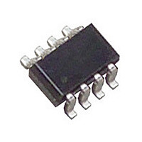
LTC2927CTS8#PBF Linear Technology, LTC2927CTS8#PBF Datasheet

LTC2927CTS8#PBF
Specifications of LTC2927CTS8#PBF
Available stocks
Related parts for LTC2927CTS8#PBF
LTC2927CTS8#PBF Summary of contents
Page 1
... FB node. Furthermore, it presents a high impedance when power-up is complete, effectively removing it from the DC/DC circuit. , LT, LTC and LTM are registered trademarks of Linear Technology Corporation. ThinSOT is a trademark of Linear Technology Corporation. All other trademarks are the property of their respective owners. Patents Pending. 0.1μF V 0.1μ ...
Page 2
... EXPOSED PAD (PIN 9) PCB GND, CONNECTION OPTIONAL = 125°C, θ 76°C/W JMAX JA ORDER INFORMATION LEAD FREE FINISH TAPE AND REEL LTC2927CDDB#PBF LTC2927CDDB#TRPBF LTC2927IDDB#PBF LTC2927IDDB#TRPBF LTC2927CTS8#PBF LTC2927CTS8#TRPBF LTC2927ITS8#PBF LTC2927ITS8#TRPBF LEAD BASED FINISH TAPE AND REEL LTC2927CDDB LTC2927CDDB#TR LTC2927IDDB LTC2927IDDB#TR LTC2927CTS8 LTC2927CTS8#TR LTC2927ITS8 LTC2927ITS8#TR Consult LTC Marketing for parts specifi ...
Page 3
ELECTRICAL CHARACTERISTICS temperature range, otherwise specifi cations are at T SYMBOL PARAMETER V Supply Voltage CC I Supply Current CC V Supply Undervoltage Lockout CC(UVLO) ΔV Supply Undervoltage Lockout Hysteresis CC(UVHYST Pin Threshold Voltage ON(TH) ΔV ON Pin ...
Page 4
LTC2927 W U TYPICAL PERFOR A CE CHARACTERISTICS V vs Temperature ON(TH) 1.240 1.235 1.230 1.225 1.220 1.215 1.210 –50 – TEMPERATURE (°C) 2927 G04 MAX TRACK TRACK ...
Page 5
CTIO S TSOT/DFN Packages GND (Pin 4/Pin 5): Device Ground. TRACK (Pin 5/Pin 4): Tracking Control Input. A resistive voltage divider between RAMPBUF and TRACK determines the tracking profi the slave supply. TRACK ...
Page 6
LTC2927 U U APPLICATIO S I FOR ATIO Power Supply Tracking and Sequencing The LTC2927 handles a variety of power-up profi les to satisfy the requirements of digital logic circuits including FPGAs, PLDs, DSPs and microprocessors. These require- ments fall ...
Page 7
U U APPLICATIO S I FOR ATIO pin is mirrored at the FB pin to establish a voltage at the output of the slave supply. The slave output voltage varies with the master signal, enabling the slave supply to be ...
Page 8
LTC2927 U U APPLICATIO S I FOR ATIO EARLY V IN 3.3V 0.1μF R ONB 138k RAMP C R RAMP ONA 10pF 100k LTC2927 SDO RUN/SS RAMPBUF 1.235V TB 16.5k TRACK R R ...
Page 9
U U APPLICATIO S I FOR ATIO Coincident Tracking Example 1V/DIV A typical application is shown in Figure 10. The master signal is a 3.3V ramp generated by the LTC2927. The slave 1 supply is a 1.8V switching power supply ...
Page 10
LTC2927 U U APPLICATIO S I FOR ATIO Ratiometric Tracking Example 1V/DIV 10ms/DIV This example converts the coincident tracking example to the ratiometric tracking profi le shown in Figure 11. The ramp rate of the master signal remains unchanged (Step ...
Page 11
U U APPLICATIO S I FOR ATIO Offset Tracking Example 1V/DIV 10ms/DIV Converting the circuit in the coincident tracking example to the offset tracking shown in Figure 13 is relatively simple. Here the 1.8V slave 1 supply ramps up 1V ...
Page 12
LTC2927 U U APPLICATIO S I FOR ATIO Supply Sequencing Example 1V/DIV 10ms/DIV In Figure 15, the slave 1 supply and the slave 2 supply are sequenced instead of tracking. The 3.3V master ramps up at 100V/s. The 1.8V slave ...
Page 13
U U APPLICATIO S I FOR ATIO Final Sanity Checks The collection of equations below is useful for identifying unrealizable solutions. As stated in step 2, the slave supply must fi nish ramping before the master signal has reached its ...
Page 14
LTC2927 U U APPLICATIO S I FOR ATIO Start-Up Delays Often power supplies do not start-up immediately when their input supplies are applied. If the LTC2927 tries to ramp-up these power supplies as soon as the input sup- ply is ...
Page 15
... MOLD FLASH SHALL NOT EXCEED 0.254mm 6. JEDEC PACKAGE REFERENCE IS MO-193 Information furnished by Linear Technology Corporation is believed to be accurate and reliable. However, no responsibility is assumed for its use. Linear Technology Corporation makes no representation that the interconnection of its circuits as described herein will not infringe on existing patent rights. U DDB Package 8-Lead Plastic DFN (3mm × ...
Page 16
... Dual Hot Swap Controller LTC4230 Triple Hot Swap Controller with Multifunction Current Control LTC4253 –48V Hot Swap Controller and Supply Sequencer Hot Swap is a trademark of Linear Technology Corporation. Linear Technology Corporation 16 1630 McCarthy Blvd., Milpitas, CA 95035-7417 (408) 432-1900 FAX: (408) 434-0507 ● ...


