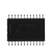
MCZ33298EGR2 Freescale, MCZ33298EGR2 Datasheet - Page 15

MCZ33298EGR2
Manufacturer Part Number
MCZ33298EGR2
Description
Manufacturer
Freescale
Datasheet
1.MCZ33298EGR2.pdf
(28 pages)
Specifications of MCZ33298EGR2
Switch Type
Low Side
Power Switch Family
MCZ33298
Input Voltage
-0.3 to 7V
Power Switch On Resistance
400mOhm
Output Current
1A
Number Of Outputs
8
Mounting
Surface Mount
Supply Current
1uA
Package Type
SOIC W
Operating Temperature (min)
-40C
Operating Temperature Classification
Automotive
Pin Count
24
Power Dissipation
3W
Lead Free Status / RoHS Status
Compliant
Available stocks
Company
Part Number
Manufacturer
Quantity
Price
Part Number:
MCZ33298EGR2
Manufacturer:
FREESCALE
Quantity:
20 000
CHIP SELECT (CS)
CS pin. Whenever this pin is in a logic low state, data can be
transferred from the MCU to the 33298 by way of the SI pin
and from the 33298 to the MCU through the SO pin. Clocked-
in data from the MCU is transferred from the 33298 Shift
register and latched into the power outputs on the rising edge
of the CS signal. On the falling edge of the CS signal, drain
status information is transferred from the power outputs then
loaded into the Shift register of the device. The CS pin also
controls the output driver of the serial output (SO) pin.
Whenever the CS pin goes to a logic low state, the SO pin
output driver is enabled allowing information to be transferred
from the 33298 to the MCU. To avoid data corruption or the
generation of spurious data, it is essential the high-to-low
transition of the CS signal occur only when SCLK is in a logic
low state.
SYSTEM CLOCK (SCLK)
registers of the 33298. The serial input (SI) pin accepts data
into the Input Shift register on the falling edge of the SCLK
signal while the serial output (SO) pin shifts data information
out of the SO line driver on the rising edge of the SCLK signal.
False clocking of the Shift register must be avoided to
guarantee validity of data. It is essential the SCLK pin be in a
logic low state whenever the chip select bar (CS) pin makes
Analog Integrated Circuit Device Data
Freescale Semiconductor
The 33298 receives its MCU communication through the
The system clock (SCLK) pin clocks the internal shift
V
V
DD
DD
Microcontroller
Microcontroller
B0
B1
SS
(Alternate Master)
B0
B1
SS
FUNCTIONAL PIN DESCRIPTION
Figure 16. Multiple MCU SPI Control
8-Bit
8-Bit
MC68XX
(Master)
MC68XX
Parallel
Parallel
Ports
Ports
SPI
SPI
SCLK
MISO
MOSI
SCLK
MISO
MOSI
A0
A1
A2
A0
A1
A2
any transition. For this reason, it is recommended, though not
absolutely necessary, the SCLK pin be kept in a low logic
state as long as the device is not accessed (CS in logic high
state). When CS is in a logic high state, signals at the SCLK
and SI pins are ignored and SO is tri-stated (high-
impedance). See the Data Transfer Timing diagram in
Figure
SERIAL INPUT (SI)
read on the falling edge of SCLK. A logic high state present
on this pin when the SCLK signal rises will program a specific
output OFF. In turn, the pin turns OFF the specific output on
the rising edge of the CS signal. Conversely, a logic low state
present on the SI pin will program the output ON, In turn, the
pin turns ON the specific output on the rising edge of the CS
signal.
8-bit serial stream of data is required to be synchronously
entered into the SI pin starting with Output 7, followed by
Output 6, Output 5, and so on, to Output 0. Referring to
Figure
corresponding to Output 7. For each rise of the SCLK signal,
with CS held in a logic low state, a data-bit instruction (ON or
OFF) is synchronously loaded into the Shift register per the
data-bit SI state. The Shift register is full after eight bits of
information have been entered. To preserve data integrity,
This pin is for the input of serial instruction (SI) data. SI is
To program the eight outputs of the 33298 ON or OFF, an
18.
18, the DO bit is the most significant bit (MSB)
CS
SCLK
SO
SI
CS
SCLK
SO
SI
CS
SCLK
SO
SI
33298
33298
33298
8-Bit
8-Bit
8-Bit
8 Outputs
8 Outputs
8 Outputs
FUNCTIONAL DESCRIPTION
INTRODUCTION
33298
15


