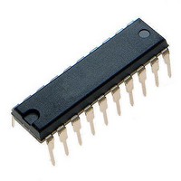
ATF16V8BQ-10PC Atmel, ATF16V8BQ-10PC Datasheet - Page 8

ATF16V8BQ-10PC
Manufacturer Part Number
ATF16V8BQ-10PC
Description
EEPLD - Electronically Erasable Programmable Logic Devices 250 GATE QRTR PWR- 10NS QTR PWR
Manufacturer
Atmel
Datasheet
1.ATF16V8BQ-10PC.pdf
(26 pages)
Specifications of ATF16V8BQ-10PC
Family Name
ATF16V8BQ
Process Technology
CMOS
# Macrocells
8
# I/os (max)
8
Frequency (max)
83MHz
Propagation Delay Time
10ns
Operating Supply Voltage (typ)
5V
Operating Supply Voltage (min)
4.75V
Operating Supply Voltage (max)
5.25V
Operating Temp Range
0C to 70C
Operating Temperature Classification
Commercial
Mounting
Through Hole
Pin Count
20
Supply Current
40mA
Delay Time
10 ns
Logic Family
ATF16V8BQ
Maximum Operating Frequency
83 MHz
Maximum Operating Temperature
+ 70 C
Minimum Operating Temperature
0 C
Mounting Style
Through Hole
Number Of Macrocells
8
Number Of Product Terms Per Macro
8
Number Of Programmable I/os
8
Operating Supply Voltage
5 V
Package / Case
PDIP-20
Supply Voltage (max)
5.25 V
Supply Voltage (min)
4.75 V
Lead Free Status / RoHS Status
Not Compliant
6. Electronic Signature Word
7. Programming/Erasing
8. Input and I/O Pull-ups
9. Functional Logic Diagram Description
8
ATF16V8B/BQ/BQL
There are 64 bits of programmable memory that are always available to the user, even if the
device is secured. These bits can be used for user-specific data.
Programming/erasing is performed using standard PLD programmers. See CMOS PLD Pro-
gramming Hardware and Software Support for information on software/programming.
All ATF16V8B family members have internal input and I/O pull-up resistors. Therefore, when-
ever inputs or I/Os are not being driven externally, they will float to V
logic array inputs are at known states. These are relatively weak active pull-ups that can easily
be overdriven by TTL-compatible drivers (see input and I/O diagrams below).
Figure 8-1.
Figure 8-2.
The Logic Option and Functional Diagrams describe the ATF16V8B architecture. Eight config-
urable macrocells can be configured as a registered output, combinatorial I/O, combinatorial
output, or dedicated input.
The ATF16V8B can be configured in one of three different modes. Each mode makes the
ATF16V8B look like a different device. Most PLD compilers can choose the right mode automat-
ically. The user can also force the selection by supplying the compiler with a mode selection.
The determining factors would be the usage of register versus combinatorial outputs and dedi-
cated outputs versus outputs with output enable control.
The ATF16V8B universal architecture can be programmed to emulate many 20-pin PAL
devices. These architectural subsets can be found in each of the configuration modes described
Input Diagram
I/O Diagram
CC
. This ensures that all
0364J–PLD–7/05


